wafer.space Run 2
40 public designs on one GF180MCU reticle
Reserve a slot on wafer.space Run 3 Or start with Tiny Tapeout
What was built
The run as a whole: what its designs add up to.
40
Public designs
in 43 of the reticle's 54 slot positions
36
Open source
with a public repository and an open licence
58.5M
Transistors
across the unique designs
2.4M
Logic cells
gates and flip-flops
152 KiB
SRAM
in foundry and custom macros
13
Whole dies
and 30 half and quarter slots
Private designs on the reticle are not in the public layout and are not counted. Designs placed more than once are counted once.
Make a chip of your own
Start small with a Tiny Tapeout tile, or go straight to a whole die on the next wafer.space run.
Make a whole chip of your own
Book a die to itself on wafer.space Run 3: orders close 9 December 2026.
Reserve a slotOr start with a Tiny Tapeout tile
Tiny Tapeout GF 26c and 26d take projects until 7 December 2026, to be made on wafer.space Run 3.
Submit a projectGet a Tiny Tapeout chip
Every Tiny Tapeout chip comes on a board you can plug in, with all of its projects ready to try.
Buy a chip and boardThe reticle
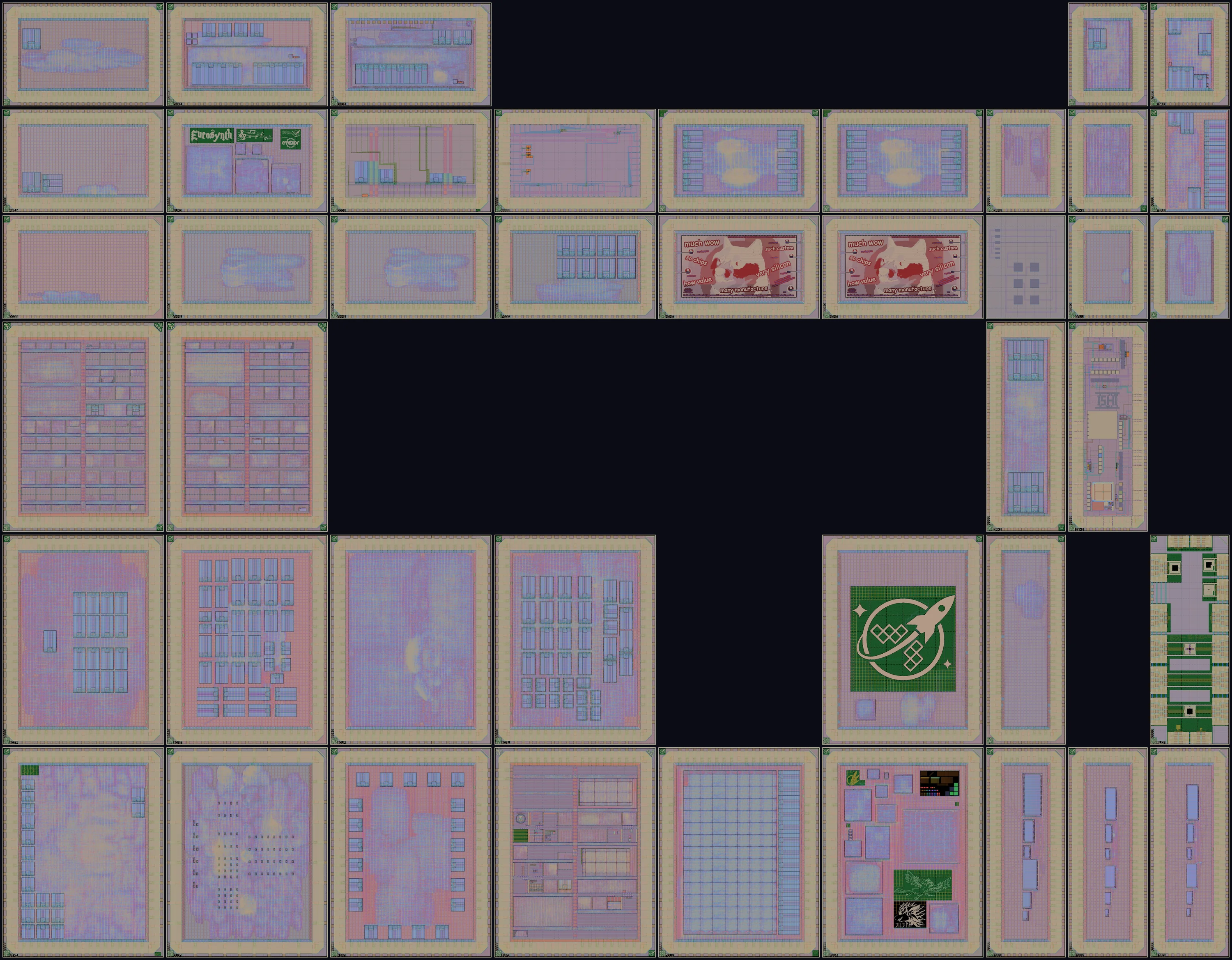 A5 · BTX1
A4 · SCTP
A3 · T26A
A2 · DCO0
A2 · AS16
A1 · TQVC
B5 · CLON
B4 · SCMT
B3 · T26B
B2 · AMM1
B2 · EURO
B1 · NAX1
C5 · KIAN
C4 · SCUP
C2 · AMM1
C2 · OCD3
C1 · CAB1
D5 · T0P3
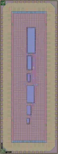
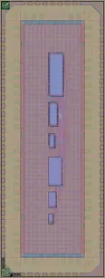
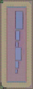
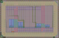
D4 · SCML
D2 · PSOC
D2 · 0000
E5 · MOLE
E2 · MEME
E2 · GD04
F5 · AS04
F4 · WSLG
F2 · MEME
F2 · GD04
G5 · FS03
G4 · HZ80
G3 · DPK1
G2 · FC01
G2 · CAFE
G5 · FS02
G3 · ISHI
G2 · SALU
G2 · DPK2
G1 · TQVA
H5 · FS01
H4 · RLCM
H2 · QZ80
H2 · TQVE
H1 · TQVD
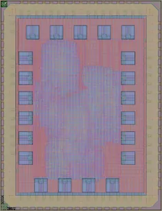
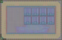
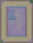
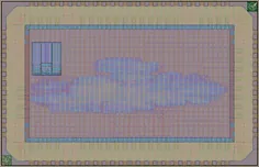
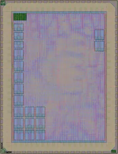
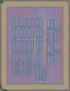
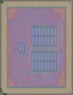
Every design rendered from the layout at the same scale and placed where it sits on the 30 × 23.4 mm reticle. Dark gaps are private designs or empty slots. Point at a die to see its name, and select it for its details.Every die is listed further down.
Slots
How much of the reticle each design took: a 1 × 1 slot is a whole die of its own, and the ½ sizes are halves and quarters of one. Some designs are placed more than once, so 40 designs fill 43 slots.
| 1 × 1 | 13 |
| 1 × ½ | 15 |
| ½ × 1 | 7 |
| ½ × ½ | 8 |
| Total | 43 |
|---|
Shuttle status
Where this run is now, from opening orders to shipping parts.
Done so far
- 1 March 2026 Campaign opens Run 2 slots available for purchase on Crowd Supply
- 30 April 2026, 23:59 AoE Early bird deadline Last day to purchase at early bird pricing
- 30 June 2026, 23:59 AoE Purchase deadline Final deadline to purchase slots
- 14 July 2026, 23:59 AoE Submission deadline Final deadline to submit clean GDS
- 22 July 2026 Tape-out to GlobalFoundries GDS files delivered to GlobalFoundries for fabrication
- 30 July 2026 Masks released Masks approved and fabrication started
- 17 September 2026 First wafers returned An initial set of wafers back from GlobalFoundries
- 8 October 2026 First wafers diced The initial wafers cut into individual dies
Still to come
- Today, 24 October 2026
- 22 October 2026 (expected) First dies sorted Dies from the initial wafers picked and sorted by project
- 22 October 2026 (expected) First bare dies shipped Initial bare dies shipped to customers
- 12 November 2026 (expected) First packaged parts shipped Initial chip-on-board packaged parts shipped
- 10 December 2026 (expected) Main wafer lot returned The first full lot of Run 2 wafers back from GlobalFoundries
- 31 December 2026 (expected) Main lot bare dies shipped Bare dies from the main lot shipped to customers
- 15 January 2027 (expected) Last wafer lot returned The rest of the Run 2 wafers back from GlobalFoundries
- 21 January 2027 (expected) Main lot packaged parts shipped Chip-on-board packaged parts from the main lot shipped
- 5 February 2027 (expected) Last lot bare dies shipped Bare dies from the last lot shipped to customers
- 26 February 2027 (expected) Last lot packaged parts shipped Chip-on-board packaged parts from the last lot shipped
Missed this run? wafer.space Run 3 takes orders until 9 December 2026: reserve a slot.
From the wafer.space run schedule.
How people used their silicon
Where the area of 40 dies (490 mm² of silicon) actually went
- Logic cells 13% — gates and flip-flops doing the design's actual work
- SRAM 6% — memory macros
- Filler and tap cells 25% — inserted by the tools to keep rows continuous and wells tied
- Other 11% — routing channels, analog and custom layout, power grid and empty space
- Pad ring 44% — the 442 µm border of I/O cells and bond pads
What people built
The kinds of design on this run.
RISC-V and CPUs 9 Multi-project die 5 Other digital 5 Memory test chip 4 Accelerators 4 Analog and mixed-signal 3 Retro computing 3 Art and logos 2 Test structures 2 FPGA 1 Security 1 Communications 1Standard cell libraries
The ready-made gate libraries the designs were built from: how many tracks tall each cell is, and the voltage it runs at.
| Standard cell library | Logic cells | Share |
|---|---|---|
| AS 7t-3.3V gf180mcu_as_sc_mcu7t3v3 | 1.3M | 53% |
| 7t-5V gf180mcu_fd_sc_mcu7t5v0 | 1.1M | 45% |
| 9t-5V gf180mcu_fd_sc_mcu9t5v0 | 46k | 2% |
| AS extra 7t-5V gf180mcu_as_ex_mcu7t5v0 | 2k | <1% |
Area budget of every design
Each bar is one die, split the same way as above. Sorted by how much of the die is logic.
Show all 40 dies
Which parts of the process were used
Transistor voltages and optional devices across the 40 designs
Transistor voltages
A design counts for a voltage when its standard cells, SRAM or its own transistors use it. 5 V and 6 V transistors share the thick gate oxide; a marker layer in the layout tells them apart.
Optional devices drawn by designers
Not drawn by any design: Native transistors, 10 V LDMOS, N-well resistors, Metal resistors, Well diodes, Zener diodes, eFuses, One-time programmable memory, Inductors.
Only devices outside standard cells, SRAM macros and I/O pads count, since every die has those. A single test structure counts the same as a large block. Faded names have the device only inside a reused block; hover over one to see which.
Gate oxides
| Transistors | Own design | With the pad ring | Which (own design) |
|---|---|---|---|
| 3.3 V and 5 V/6 V | 9 | 20 | |
| 3.3 V only | 11 | 0 | |
| 5 V/6 V only | 18 | 18 | 18 designsraybox-zero wafer.space run 2 half height, 16-bit RISC CPU, Expresso Ethernet Chip: 100Mbps Ethernet switch + Heat death of the Universe Beacon - 0.5x0.5 version - Preferred version, Cloneless2, Standard Cell DCO+TDC, bio180, cordic-romless-x8, EuroSynth, Test chip with 5V SRAM blocks, Racquet Wide 1x0.5, FOSSi open-source replacement for Z80 classic 8-bit CPU (0.5 x 1 slot), Artwork Meme Chip, Simplest possible PicoSoC implementation using wafer.space flow, FOSSi open-source replacement for Z80 classic 8-bit CPU (0.5 x 0.5 slot), Simple ALU, TinyQV - Crowdsourced RISC-V SoC, TinyQV - Crowdsourced RISC-V SoC (1x0.5), wafer.space Logo |
3.3 V transistors have the thin gate oxide; 5 V and 6 V ones share the thick one. "Own design" counts the standard cells, SRAM and transistors the designer chose; "with the pad ring" adds the transistors of the I/O pad cells, measured in each design's pad ring. No transistors of their own: Flip Chip pad test version 1, RLCM: Test Passives For GF180MCUD.
Licences
The licence each designer declared when submitting.
| Declared licence | Designs |
|---|---|
| Apache-2.0 | 29 |
| MIT | 3 |
| CERN-OHL-S-2.0 | 2 |
| CERN-OHL-P-2.0 | 2 |
| GPL-3.0-only | 1 |
| BSD-3-Clause | 1 |
| proprietary | 1 |
| GPL-3.0-or-later | 1 |
Some repositories carry a different licence file from the one declared at submission, or none: check a design's repository, and its page here, before reusing it.
Packaging and precheck
How the designs will be packaged, and whether they passed the design-rule checks before manufacture.
- 24 of 40 designs selected chip-on-board packaging.
- 39 of 40 designs passed the platform precheck they were accepted on (2026-07-04 to 2026-07-16), and 39 pass their latest re-run; FC01 has no finished precheck recorded.
- The KLayout DRC, the sign-off check, is clear in every one of these checks.
- The chip-on-board pad mask check passed for all 25 designs that ran it (AS16 switched chip-on-board off after the check it was accepted on).
- The advisory Magic DRC reported errors for CAB1, FS01, FS02, FS03, GD04, RLCM, T0P3, T26A, T26B.
What fits on 1 mm² of GF180MCU silicon?
Theoretical maximum against what designers achieved
The maximum packs one cell type edge to edge with no room for wiring. Real designs need the wiring. Each box gives the most of a cell that fits with any GF180MCU library, then with the libraries this run used.
~114k
Inverters per mm²
GF180MCU maximum,
with
AS 7t-3.3V
inv_2
With this run's libraries:
AS 7t-3.3V: 114k inv_2
~76k
Buffers per mm²
GF180MCU maximum,
with
AS 7t-3.3V
buff_2
With this run's libraries:
AS 7t-3.3V: 76k buff_2
~17k
Flip-flops per mm²
GF180MCU maximum,
with
AS 7t-3.3V
dfxtp_2
With this run's libraries:
AS 7t-3.3V: 17k dfxtp_2
AS extra 7t-5V: 14k dfxtp_2
8k
Typical die
median logic cells/mm² of core across 34 digital dies (1,000 or more logic cells)
26% of the core covered by logic cells
Percentages compare with the buffer maximum for each design's own library: buffers are among the smallest and most common logic cells, so a design made only of buffers, packed edge to edge with no wiring, would reach 100%.
Sizing your own design
What each slot size held on this run, and what it would hold at its densities
| Logic cells in its digital designs1,000 or more logic cells | Logic cells at this run's density | Theoretical maximum, AS 7t-3.3V cells | ||||||||
|---|---|---|---|---|---|---|---|---|---|---|
| Slot | Die | Core area | Designs | Most | Median | Typical8k / mm² | Best25k / mm² | Densest34k / mm² | NAND gatesnand2_2 | Flip-flopsdfxtp_2 |
| 1 × 1 | 3.93 × 5.12 mm | 12.9 mm² | 13 | 324k | 125k | 102k | 324k | 439k | 841k | 218k |
| 1 × ½ | 3.93 × 2.53 mm | 5.0 mm² | 12 | 68k | 36k | 40k | 126k | 170k | 326k | 85k |
| ½ × 1 | 1.94 × 5.12 mm | 4.5 mm² | 7 | 66k | 4k | 35k | 112k | 151k | 290k | 75k |
| ½ × ½ | 1.94 × 2.53 mm | 1.7 mm² | 8 | 36k | 24k | 14k | 43k | 59k | 113k | 29k |
Swipe the table sideways for more columns.
Core area is each design's CORE_AREA, read from its own LibreLane config at the commit that was checked; where that could not be read, the project template's, 442 µm in from each edge of the die. Density inside the seal ring is over the whole die less its 26 µm seal ring: all the silicon a slot gives its designer, pad ring included. "Typical" and "best" multiply the core area by this run's median and best core densities, and "densest" by the densest 1 mm² any design on this run reached; SRAM and analog blocks take their area out of that. The theoretical maxima fill the core with nothing but that one cell of AS 7t-3.3V, the library most used on this run, edge to edge with no routing.
Pick the slot size your design needs on wafer.space Run 3: orders close 9 December 2026.
Logic density of every digital design
A digital die here is one with 1,000 or more logic cells. Solid bar: average over the core. Dark line inside it: average over all the silicon inside the seal ring, pad ring included. Outlined bar: the densest mm² outside SRAM (a dash where memory covers most of the design). The scale ends at the buffer theoretical maximum (76k cells/mm²). The numbers are core / seal ring / densest, in logic cells per mm².
Show all 34 digital dies
Every digital die's densities as a table
| Design | Slot | Library | Logic cells | Inside core per mm² |
Inside seal ring per mm² | Densest mm² per mm² |
Core covered | Core mm² |
|---|---|---|---|---|---|---|---|---|
| Cloneless2 CLON | 1 × 1 | 7t-5V | 323,612 | 25,081 | 16,466 | 29,930 | 58% | 12.90* |
| TinyQV - Crowdsourced RISC-V SoC TQVA | ½ × ½ | 7t-5V | 35,711 | 20,611 | 7,633 | 22,636 | 47% | 1.73 |
| BTX BTX1 | 1 × 1 | AS 7t-3.3V | 252,619 | 19,579 | 12,854 | 24,790 | 47% | 12.90* |
| cordic-romless-x8 DPK2 | ½ × ½ | 7t-5V | 33,464 | 19,314 | 7,153 | 21,060 | 40% | 1.73 |
| GF180MCU Peripherals SCUP | 1 × 1 | AS 7t-3.3V | 239,123 | 18,512 | 12,167 | 33,972 | 53% | 12.92 |
| FABulous FPGA MOLE | 1 × 1 | AS 7t-3.3V | 211,813 | 16,397 | 10,777 | 24,122 | 53% | 12.92 |
| bio180 DPK1 | ½ × 1 | 7t-5V | 66,232 | 14,856 | 6,922 | 26,918 | 33% | 4.46 |
| TinyQV - RISC-V SoC with experimental pad setup TQVE | ½ × ½ | AS 7t-3.3V | 24,213 | 13,930 | 5,175 | 15,896 | 40% | 1.74* |
| TinyQV - RISC-V SoC with HDMI output TQVD | ½ × ½ | AS 7t-3.3V | 23,689 | 13,672 | 5,063 | — | 37% | 1.73 |
| EuroSynth EURO | 1 × ½ | 7t-5V | 68,077 | 13,561 | 7,084 | 27,030 | 34% | 5.02 |
| Tiny Tapeout GF 26b T26B | 1 × 1 | mixed | 155,961 | 12,087 | 7,935 | 24,556 | 35% | 12.90* |
| Tiny Tapeout GF 26a T26A | 1 × 1 | 7t-5V | 144,419 | 11,193 | 7,348 | 22,754 | 33% | 12.90* |
| Cabrera CoB CAB1 | 1 × ½ | 7t-5V | 52,199 | 10,398 | 5,432 | 18,627 | 29% | 5.02 |
| Naxos CoB NAX1 | 1 × ½ | AS 7t-3.3V | 49,919 | 9,944 | 5,195 | — | 27% | 5.02 |
| SlugTPU SCTP | 1 × 1 | AS 7t-3.3V | 124,628 | 9,648 | 6,341 | 14,116 | 26% | 12.92 |
| Tiny Tapeout GF 0.3 T0P3 | 1 × 1 | mixed | 118,911 | 9,216 | 6,050 | 24,632 | 27% | 12.90* |
| ML-Audio SC SCML | 1 × 1 | AS 7t-3.3V | 111,492 | 8,631 | 5,673 | 13,251 | 25% | 12.92 |
| TinyQV - Crowdsourced RISC-V SoC (1x0.5) TQVC | 1 × ½ | 7t-5V | 36,116 | 7,194 | 3,758 | 16,157 | 16% | 5.02 |
| Racquet Wide 1x0.5 GD04 | 1 × ½ | 9t-5V | 35,525 | 7,077 | 3,697 | 18,167 | 28% | 5.02 |
| Multi-Project die using 3.3V SCL AS04 | 1 × 1 | AS 7t-3.3V | 87,322 | 6,760 | 4,443 | 18,663 | 18% | 12.92 |
| raybox-zero wafer.space run 2 half height AMM1 | 1 × ½ | 7t-5V | 31,608 | 6,296 | 3,289 | 18,587 | 19% | 5.02 |
| KianV: A 32-bit RISC-V Linux SoC taped out on GF180MCU Run 2 KIAN | 1 × 1 | AS 7t-3.3V | 76,850 | 5,949 | 3,910 | 14,729 | 16% | 12.92 |
| Expresso Ethernet Chip: 100Mbps Ethernet switch + Heat death of the Universe Beacon - 0.5x0.5 version - Preferred version CAFE | ½ × ½ | 7t-5V | 8,747 | 5,048 | 1,870 | 7,693 | 15% | 1.73 |
| microTheia SCMT | 1 × 1 | AS 7t-3.3V | 47,523 | 3,679 | 2,418 | — | 7% | 12.92 |
| Simplest possible PicoSoC implementation using wafer.space flow PSOC | 1 × ½ | 7t-5V | 18,372 | 3,660 | 1,912 | — | 11% | 5.02 |
| FOSSi open-source replacement for Z80 classic 8-bit CPU (0.5 x 0.5 slot) QZ80 | ½ × ½ | 9t-5V | 5,096 | 2,941 | 1,089 | 4,090 | 10% | 1.73 |
| Standard Cell DCO+TDC DCO0 | 1 × ½ | 7t-5V | 7,139 | 1,422 | 743 | 5,147 | 6% | 5.02 |
| FOSSi open-source replacement for Z80 classic 8-bit CPU (0.5 x 1 slot) HZ80 | ½ × 1 | 9t-5V | 5,143 | 1,154 | 537 | 4,951 | 4% | 4.46 |
| wafer.space Logo WSLG | 1 × 1 | mixed | 14,290 | 1,106 | 727 | 11,110 | 4% | 12.92 |
| 16-bit RISC CPU AS16 | 1 × ½ | 7t-5V | 5,508 | 1,097 | 573 | 5,430 | 4% | 5.02 |
| Simple ALU SALU | ½ × ½ | 7t-5V | 1,608 | 928 | 344 | 1,592 | 3% | 1.73 |
| Test chip with 5V SRAM blocks FS03 | ½ × 1 | 7t-5V | 3,788 | 847 | 396 | 1,789 | 2% | 4.47* |
| Test chip with 3.3V SRAM blocks using regular design rules FS01 | ½ × 1 | 7t-5V | 3,540 | 791 | 370 | 1,845 | 2% | 4.47* |
| Test chip with 3.3V SRAM blocks using SRAM design rules FS02 | ½ × 1 | 7t-5V | 3,492 | 781 | 365 | 1,807 | 2% | 4.47* |
* The project template's core: the design's own config could not be read.
The projects
Every design on this run: an index, then grouped by what it does. Select one for its layout, its measurements and any die photographs.
Design index
All 40 public designs by their code, with the slot each took and how much logic it packs.
Swipe the table sideways for more columns.
Designs that grew
These designs have been made more than once: first as a Tiny Tapeout tile or on a Google shuttle, then on wafer.space, or improved and made again on a later run. Start small, then come back bigger. The ringed marker is this run.
56C6 One-hot FABulous FPGA
Caravel chip wafer.space Run 1 · Dec 2025
MOLE FABulous FPGA
1 × 1 slot Tiny Tapeout IHP 26a · Mar 2026
Tiny FABulous FPGA
8 × 4 tiles Tiny Tapeout SKY 26a · May 2026
Tiny FABulous FPGA
8 × 4 tiles Tiny Tapeout SKY 26b · May 2026
Tiny FABulous FPGA
8 × 4 tiles Tiny Tapeout GF 0.3 · Jun 2026
2 projects
4 × 4 tiles wafer.space Run 2 · Jul 2026
MOLE FABulous FPGA
1 × 1 slot Tiny Tapeout SKY 26c · Sep 2026
Tiny FABulous FPGA
8 × 4 tiles Tiny Tapeout IHP 26b · Sep 2026
Tiny FABulous FPGA
6 × 4 tiles
TinyQV RISC-V SoC
2 × 2 tiles Tiny Tapeout IHP 0.2 · Nov 2024
TinyQV RISC-V SoC
2 × 2 tiles Tiny Tapeout IHP 25a · Mar 2025
TinyQV RISC-V SoC
3 × 2 tiles Tiny Tapeout IHP 25b · Sep 2025
TinyQV - Crowdsourced RISC-V SoC
5 × 4 tiles Tiny Tapeout SKY 25a · Sep 2025
2 projects
8 × 4 tiles, 4 × 4 tiles Tiny Tapeout SKY 25b · Nov 2025
TinyQV RISC-V SoC
3 × 2 tiles Tiny Tapeout GF 0.1 · Nov 2025
TinyQV RISC-V SoC
in a shared block Tiny Tapeout GF 0.2 · Nov 2025
TinyQV RISC-V SoC
3 × 4 tiles wafer.space Run 1 · Dec 2025
3 dies
TQVA ½ × ½ slot, TQVB ½ × 1 slot, TQVC 1 × ½ slot Tiny Tapeout GF 0.3 · Jun 2026
TinyQV RISC-V SoC
4 × 2 tiles wafer.space Run 2 · Jul 2026
4 dies
TQVA ½ × ½ slot, TQVC 1 × ½ slot, TQVD ½ × ½ slot, TQVE ½ × ½ slot
KianV uLinux SoC
8 × 2 tiles Tiny Tapeout 6 · Apr 2024
KianV uLinux SoC
8 × 2 tiles Tiny Tapeout 7 · Jun 2024
KianV RISC-V RV32E Baremetal SoC
3 × 2 tiles Tiny Tapeout IHP 0.2 · Nov 2024
KianV RISC-V RV32E Baremetal SoC
4 × 2 tiles Tiny Tapeout GF 0.1 · Nov 2025
KianV uLinux SoC
in a shared block Tiny Tapeout GF 0.2 · Nov 2025
KianV uLinux SoC
4 × 4 tiles wafer.space Run 1 · Dec 2025
KIAN KianV: A 32-bit RISC-V Linux SoC taped out on GF180MCU
1 × 1 slot Tiny Tapeout IHP 26a · Mar 2026
KianV SV32 TT Linux SoC
8 × 4 tiles Tiny Tapeout GF 0.3 · Jun 2026
KianV uLinux SoC
4 × 4 tiles wafer.space Run 2 · Jul 2026
KIAN KianV: A 32-bit RISC-V Linux SoC taped out on GF180MCU Run 2
1 × 1 slot
raybox-zero
4 × 2 tiles Tiny Tapeout 7 · Jun 2024
raybox-zero TT07 edition
6 × 2 tiles Tiny Tapeout IHP 0.2 · Nov 2024
raybox-zero TTIHP0p2 edition
4 × 2 tiles Tiny Tapeout GF 0.1 · Nov 2025
raybox-zero TT07 edition
in a shared block Tiny Tapeout GF 0.2 · Nov 2025
raybox-zero TTGF0p2 edition
3 × 4 tiles Tiny Tapeout IHP 0.4 · Mar 2026
raybox-zero TTIHP0p4 edition
6 × 2 tiles wafer.space Run 2 · Jul 2026
AMM1 raybox-zero wafer.space run 2 half height
1 × ½ slot
Zilog Z80
2 × 2 tiles Tiny Tapeout IHP 0.2 · Nov 2024
Zilog Z80
2 × 2 tiles Tiny Tapeout 9 · Nov 2024
Zilog Z80
2 × 2 tiles Tiny Tapeout IHP 25a · Mar 2025
Zilog Z80
2 × 2 tiles Tiny Tapeout GF 0.2 · Nov 2025
Zilog Z80
2 × 2 tiles wafer.space Run 1 · Dec 2025
2 dies
HZ80 ½ × 1 slot, RZ80 1 × 1 slot wafer.space Run 2 · Jul 2026
2 dies
HZ80 ½ × 1 slot, QZ80 ½ × ½ slot
serv - Serial RISC-V CPU
1 × 1 tile Google GFMPW-0 · Dec 2022
6079 Serv tri-core (GF180 MPW0 Serv)
Caravel chip Tiny Tapeout 3 · Apr 2023
serv - Serial RISC-V CPU
1 × 1 tile wafer.space Run 1 · Dec 2025
3 dies
GD02 ½ × 1 slot, GD03 1 × 1 slot, GD04 1 × ½ slot wafer.space Run 2 · Jul 2026
GD04 Racquet Wide 1x0.5
1 × ½ slot
Tiny Tapeout tile
Google shuttle
wafer.space die
this run
Each marker is one version of the design: hover over it or focus it for details, and select it to open its
page. On a phone, the table below lists every one.
As a table
3 dies are Tiny Tapeout chips
Tiny Tapeout GF 0.3 (T0P3), Tiny Tapeout GF 26a (T26A) and Tiny Tapeout GF 26b (T26B) each hold dozens of small projects from Tiny Tapeout, the cheaper way to make a first chip. Each has pages of its own, project by project.
Tiny Tapeout chips on wafer.space Submit to the next one, by 7 December 2026
RISC-V and CPUs 9
Multi-project die 5
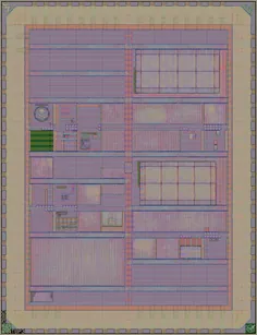
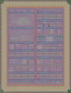
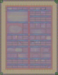
Other digital 5
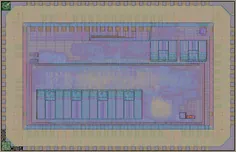
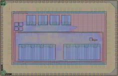
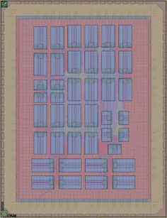
Memory test chip 4
Accelerators 4
Analog and mixed-signal 3
Retro computing 3
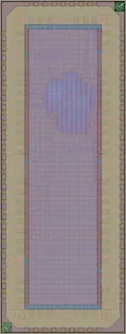
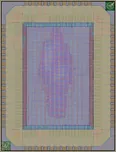
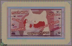
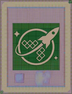
Art and logos 2
Test structures 2
FPGA 1
Security 1
Communications 1
Data and method
Everything on this page is measured from the public layout; the dates come from the published schedules.
- Logic cells are standard cell instances, excluding fillers, taps, antenna diodes and tie cells.
- Transistors are places where gate polysilicon crosses diffusion, not counting dummy fill.
- Core area is each design's CORE_AREA, read from its own LibreLane config at the commit that was checked; where that could not be read, the project template's, 442 µm in from each edge of the die. Density inside the seal ring is over the whole die less its 26 µm seal ring: all the silicon a slot gives its designer, pad ring included.
- Bond pads are the pad openings in the pad ring, or in a second ring of pads inside it for chip-on-board bonding; probe pads are the others, next to the blocks they test. Letters and logos on the pad layer are not pads.
- Theoretical maximum tiles one cell at its placement boundary with no routing.
- Densest mm² is the best 1 mm square anywhere in each die, sliding in 0.1 mm steps and avoiding SRAM.
The full written analysis is the density report. The measurements behind it:
- projects.json
- reticle_analysis.csv
- reticle_analysis_cells.csv
- reticle_analysis_content.csv
- reticle_analysis_features.csv
- reticle_analysis_grid.csv
- reticle_analysis_library.csv
- reticle_analysis_macros.csv
- reticle_analysis_map.csv
- reticle_analysis_meta.json
- reticle_analysis_metal.csv
- reticle_analysis_provenance.csv
- reticle_analysis_slot_areas.csv
- reticle_analysis_slot_macros.csv
- reticle_analysis_sram_rects.csv
- reticle_analysis_usage.csv
- reticle_analysis_windows.csv
- reticle_density_report.md
Generated by ws-run-reports from layout/G802.oas (md5 57fa57f52eac82835a051f2a353e5a30).