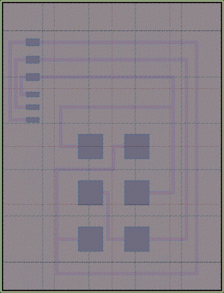
Rendered from the layout at 2.5 µm per pixel. Layers: NwellDiffusionPolysiliconMetal 1Metal 2Metal 3Metal 4Metal 5Top metalPad openings
Every figure here is measured from the public layout, the same way for every design on the run: see data and method, and how its designs used the process.
Just some test pads for flip chip bonding trials
| Die | 1.94 × 2.53 mm (4.9 mm²) |
|---|---|
| Core area | 1.74 mm² inside the pad ring
the project template's, 442 µm in from each edge |
| Inside the seal ring | 4.68 mm² (the die less its 26 µm seal ring) |
| Placements | 1 on the reticle, in slot G2 |
| Bond pads | 12 |
| Transistors | 0 |
| Logic cells | 0 |
| SRAM | No SRAM |
Submission
| Licence | Apache-2.0 declared
No public repository |
|---|---|
| Chip-on-board | Not selected at submission |
| Precheck | No finished precheck recorded |