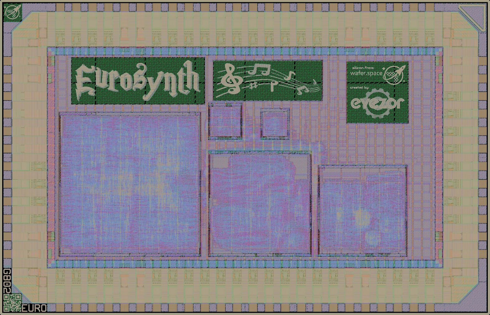
Rendered from the layout at 2.5 µm per pixel. Layers: NwellDiffusionPolysiliconMetal 1Metal 2Metal 3Metal 4Metal 5Top metalPad openings
Logic density
| Inside the core logic cells per mm² | 14k
(18% of buffer maximum) over the 5.02 mm² core: what the design itself packed |
|---|---|
| Inside the seal ring logic cells per mm² | 7k
over all 9.61 mm² of the slot, pad ring included |
| Densest mm² logic cells per mm² | 27k (36% of buffer maximum) |
| Core covered by logic | 34% |
| Transistor density transistors per mm² | 211k average, 310k in the mm² with the most logic cells |
Every figure here is measured from the public layout, the same way for every design on the run: see data and method, and how its designs used the process.
A kitchen-sink synthesizer voice in custom silicon — a fully digital eurorack synth voice taped out on the open-source GlobalFoundries 180 nm (GF180MCU) PDK with the LibreLane RTL-to-GDSII flow.
| Die | 3.93 × 2.53 mm (9.9 mm²) |
|---|---|
| Core area | 5.02 mm² inside the pad ring
as set in the design's own layout settings |
| Inside the seal ring | 9.61 mm² (the die less its 26 µm seal ring) |
| Placements | 1 on the reticle, in slot B2 |
| Bond pads | 72 |
| Transistors | 1,057,096 |
| Logic cells | 68,077 + 129,324 filler and tap cells |
| Libraries | 7t-5V (68k) |
| SRAM | No SRAM |
Submission
| Licence | Apache-2.0 declared
Repository: Apache-2.0 in LICENSE — agrees |
|---|---|
| Template | egorxe/gf180mcu-caravel-template from its README |
| How it was checked | Commit and PDK pinThe licence and template were read from the repository at commit 606cb4d8cd1e. |
| Chip-on-board | Selected at submission |
| Precheck | Passed
the check it was accepted on, 2026-07-06
Passed latest re-run, 2026-08-02, gf180mcu-precheck 1.7.3 step results and logs |
Process features
Which parts of the GF180MCU process this design uses: its transistor voltages and where they come from, its gate oxides, and any devices drawn by hand outside the standard cells, SRAM and pads.
| 5 V | 7t-5V standard cells |
|---|---|
| Gate oxides | Thick only (5 V/6 V) in the design itself |
| I/O library | gf180mcu_fd_io (758 cells) |
Where the area went
How this design's area splits between logic cells, filler and tap cells, other and pad ring.
- Logic cells 1.69 mm² (17%)
- Filler and tap cells 2.06 mm² (21%)
- Other 1.27 mm² (13%)
- Pad ring 4.92 mm² (50%)
Most used cells
The ten standard cells this design uses most.
| Cell | Library | Instances | What it does |
|---|---|---|---|
| nand2_1 | 7t-5V | 12,011 | 2-input NAND gate |
| buf_1 | 7t-5V | 6,804 | Buffer |
| oai21_1 | 7t-5V | 6,205 | OR-AND-Invert compound gate |
| dffq_1 | 7t-5V | 6,176 | D flip-flop (1 bit storage) |
| xor2_1 | 7t-5V | 3,595 | 2-input XOR gate |
| aoi21_1 | 7t-5V | 3,177 | AND-OR-Invert compound gate |
| buf_4 | 7t-5V | 2,760 | Buffer (4x drive) |
| buf_2 | 7t-5V | 2,384 | Buffer (2x drive) |
| nor2_1 | 7t-5V | 2,182 | 2-input NOR gate |
| clkbuf_8 | 7t-5V | 1,987 | Clock buffer (8x drive) |
Logic density map
Logic cells per mm² in each square millimetre of the die. Hatched outlines are SRAM macros; the red outline is the densest mm² that avoids them (27k logic cells per mm²), found by sliding a 1 mm square over the die in 0.1 mm steps, so it can straddle the fixed squares and find more than any one of them. Squares at the edges are partial, so they read low.
Precheck
Before a design is made, the wafer.space platform checks it against the foundry's design rules. EURO was accepted on this check, and has been checked again since with newer rules.
All 17 steps passed, with 0 KLayout DRC errors, on 2026-07-06.
Every step, and the latest re-run
| Step | Accepted on check 387, 2026-07-06, drc_update | Latest re-run check 748, 2026-08-02, retry, gf180mcu-precheck 1.7.3 PDK open_pdks 1.0.604, LibreLane 5fe3db1 |
|---|---|---|
| KLayout.ReadLayout | passed | passed |
| KLayout.CheckTopLevel | passed | passed |
| KLayout.CheckSize | passed | passed |
| KLayout.CheckPadMask | passed | passed |
| KLayout.GenerateID | passed | passed |
| KLayout.Render | passed | passed |
| KLayout.Density | passed | passed |
| Checker.KLayoutDensity | passed | passed |
| KLayout.ZeroAreaPolygons | passed | passed |
| Checker.KLayoutZeroAreaPolygons | passed | passed |
| KLayout.Antenna | passed | passed |
| Checker.KLayoutAntenna | passed | passed |
| Magic.DRC | passed | passed |
| Checker.MagicDRC | passed | passed |
| KLayout.DRC | passed | passed |
| Checker.KLayoutDRC | passed | passed |
| KLayout.WriteLayout | passed | passed |
| KLayout DRC errors | 0 | 0 |
| Magic DRC errors (advisory) | 0 | 0 |
| Files | steps · log (gzip) | steps · log (gzip) |
The steps of the gf180mcu-precheck LibreLane flow, as run by platform.wafer.space. The design was accepted on the newest finished check before it was submitted; later re-runs check the same file with updated rules. KLayout DRC is the sign-off check. Magic DRC is advisory: its count does not stop a design. In the logs, Magic's "Error while reading cell" lines about fill cells are messages from its reader, not check failures.