Tiny Tapeout GF 0.3Die T0P3 on wafer.space Run 2
32 projects on one chip, measured one by one and as a whole die
Buy a chip and boardPut your design on the next oneAll its projects on tinytapeout.com
What was built
The chip as a whole: what its projects add up to.
32
Projects
on the chip
32
Open source
with a public repository
1.6M
Transistors
across the unique designs
113k
Logic cells
gates and flip-flops
256 bytes
SRAM
in foundry and custom macros
Counted inside the projects only, so these totals are smaller than the die's own figures on its run's page: the pads, Tiny Tapeout's multiplexer and controller and the fill are left out.
Get this chip, or make your own
Tiny Tapeout puts many small designs on one chip. Start with a tile, then come back with a whole die.
Get a Tiny Tapeout chip
Every Tiny Tapeout chip comes on a board you can plug in, with all of its projects ready to try.
Buy a chip and boardPut your design on the next one
Tiny Tapeout GF 26c and 26d take projects until 7 December 2026, to be made on wafer.space Run 3.
Submit a projectMake a whole chip of your own
When a design outgrows a few tiles, it can have a die to itself on wafer.space Run 3: orders close 9 December 2026.
Reserve a slotThe die
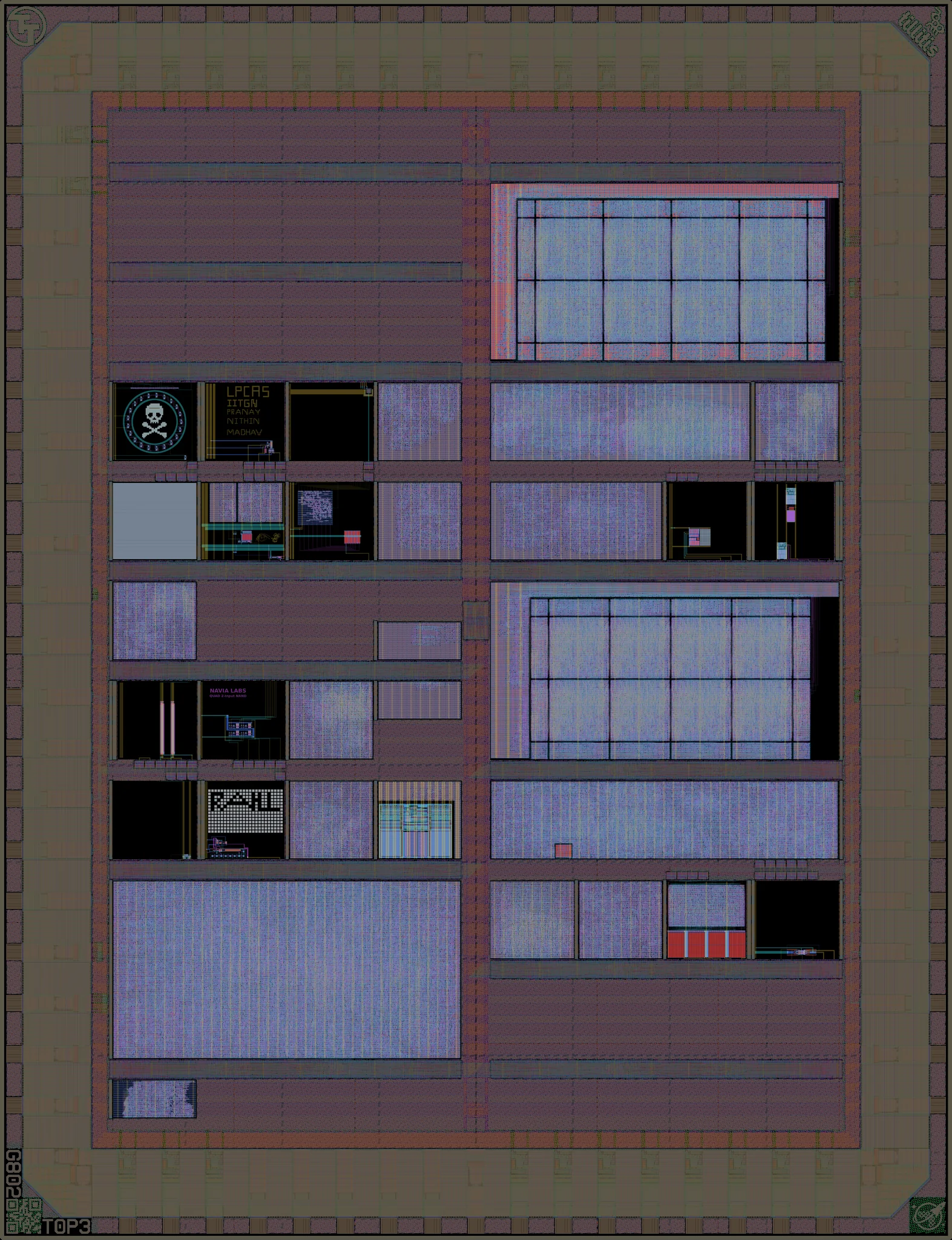
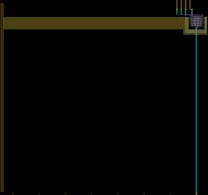
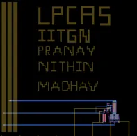
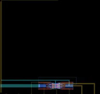
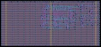
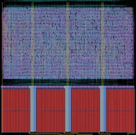
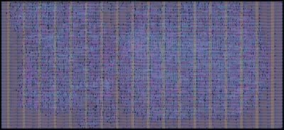
Every design rendered from the layout at the same scale and placed where it sits on the 3.9 × 5.1 mm die. Point at a project to see its name, and select it for its details.Every project is listed further down.
Project sizes
How many tiles each project took. A tile is the smallest piece of a Tiny Tapeout chip you can submit a design to.
| 1 × 1 tiles | 3 |
| 1 × 2 tiles | 23 |
| 2 × 2 tiles | 1 |
| 3 × 2 tiles | 1 |
| 4 × 2 tiles | 1 |
| 4 × 4 tiles | 3 |
| Total | 32 |
|---|
Shuttle status
Two schedules meet here: Tiny Tapeout collects the projects and builds the die, then wafer.space manufactures it on wafer.space Run 2 and ships the parts.
Done so far
- wafer.space 1 March 2026 Campaign opens Run 2 slots available for purchase on Crowd Supply
- wafer.space 30 April 2026, 23:59 AoE Early bird deadline Last day to purchase at early bird pricing, for whole-die slots on the run (not Tiny Tapeout projects)
- Tiny Tapeout 19 June 2026 Tiny Tapeout GF 0.3 submissions close Last day to submit a project to this Tiny Tapeout shuttle
- wafer.space 30 June 2026, 23:59 AoE Purchase deadline Final deadline to purchase slots, for whole-die slots on the run (not Tiny Tapeout projects)
- Tiny Tapeout 4 July 2026 Tiny Tapeout GF 0.3 tapeout release Tiny Tapeout publishes the die's layout (tapeout-ws2607) and sends it to wafer.space
- wafer.space 14 July 2026, 23:59 AoE Submission deadline Final deadline to submit clean GDS
- wafer.space 22 July 2026 Tape-out to GlobalFoundries GDS files delivered to GlobalFoundries for fabrication
- wafer.space 30 July 2026 Masks released Masks approved and fabrication started
- wafer.space 17 September 2026 First wafers returned An initial set of wafers back from GlobalFoundries
- wafer.space 8 October 2026 First wafers diced The initial wafers cut into individual dies
Still to come
- Today, 24 October 2026
- wafer.space 22 October 2026 (expected) First dies sorted Dies from the initial wafers picked and sorted by project
- wafer.space 22 October 2026 (expected) First bare dies shipped Initial bare dies shipped to customers
- wafer.space 12 November 2026 (expected) First packaged parts shipped Initial chip-on-board packaged parts shipped
- wafer.space 10 December 2026 (expected) Main wafer lot returned The first full lot of Run 2 wafers back from GlobalFoundries
- wafer.space 31 December 2026 (expected) Main lot bare dies shipped Bare dies from the main lot shipped to customers
- wafer.space 15 January 2027 (expected) Last wafer lot returned The rest of the Run 2 wafers back from GlobalFoundries
- wafer.space 21 January 2027 (expected) Main lot packaged parts shipped Chip-on-board packaged parts from the main lot shipped
- wafer.space 5 February 2027 (expected) Last lot bare dies shipped Bare dies from the last lot shipped to customers
- wafer.space 26 February 2027 (expected) Last lot packaged parts shipped Chip-on-board packaged parts from the last lot shipped
Missed this one? Tiny Tapeout GF 26c and 26d take projects until 7 December 2026: submit a project.
From the wafer.space run schedule and the Tiny Tapeout GF 0.3 repository.
How people used their silicon
Where the area of 32 projects (7 mm² of silicon) actually went
- Logic cells 46% — gates and flip-flops doing the design's actual work
- SRAM 1% — memory macros
- Filler and tap cells 26% — inserted by the tools to keep rows continuous and wells tied
- Other 27% — routing channels, analog and custom layout, power grid and empty space
What people built
The kinds of design on this chip.
Analog and mixed-signal 11 Other digital 6 FPGA 3 Security 2 Test structures 2 Games 2 RISC-V and CPUs 2 Communications 2 Art and logos 1 Retro computing 1Standard cell libraries
The ready-made gate libraries the designs were built from: how many tracks tall each cell is, and the voltage it runs at.
| Standard cell library | Logic cells | Share |
|---|---|---|
| 7t-5V gf180mcu_fd_sc_mcu7t5v0 | 88k | 78% |
| AS 7t-3.3V gf180mcu_as_sc_mcu7t3v3 | 25k | 22% |
Area budget of every design
Each bar is one project, split the same way as above. Sorted by how much of the project is logic.
Show all 32 projects
Which parts of the process were used
Transistor voltages and optional devices across the 32 designs
Transistor voltages
A design counts for a voltage when its standard cells, SRAM or its own transistors use it. 5 V and 6 V transistors share the thick gate oxide; a marker layer in the layout tells them apart.
Optional devices drawn by designers
Not drawn by any design: Native transistors, 10 V LDMOS, MIM capacitors, Salicided poly resistors, Diffusion resistors, N-well resistors, Metal resistors, Diodes, Well diodes, Schottky diodes, Zener diodes, eFuses, One-time programmable memory, Inductors.
Only devices outside standard cells, SRAM macros and I/O pads count, since every die has those. A single test structure counts the same as a large block.
Gate oxides
3.3 V transistors have the thin gate oxide; 5 V and 6 V ones share the thick one. No transistors of their own: MoM capacitor.
What fits on 1 mm² of GF180MCU silicon?
Theoretical maximum against what designers achieved
The maximum packs one cell type edge to edge with no room for wiring. Real designs need the wiring. Each box gives the most of a cell that fits with any GF180MCU library, then with the libraries this chip used.
~114k
Inverters per mm²
GF180MCU maximum,
with
AS 7t-3.3V
inv_2
With this chip's libraries:
AS 7t-3.3V: 114k inv_2
~76k
Buffers per mm²
GF180MCU maximum,
with
AS 7t-3.3V
buff_2
With this chip's libraries:
AS 7t-3.3V: 76k buff_2
~17k
Flip-flops per mm²
GF180MCU maximum,
with
AS 7t-3.3V
dfxtp_2
With this chip's libraries:
AS 7t-3.3V: 17k dfxtp_2
28k
Best core average
logic cells/mm² of core — 37% of the buffer maximum
20k
Typical project
median logic cells/mm² of core across 16 digital projects (1,000 or more logic cells)
58% of the core covered by logic cells
Percentages compare with the buffer maximum for each design's own library: buffers are among the smallest and most common logic cells, so a design made only of buffers, packed edge to edge with no wiring, would reach 100%.
Sizing your own design
What each tile size held on this chip, and what it would hold at its densities
| Logic cells in its digital projects1,000 or more logic cells | Logic cells at this chip's density | Theoretical maximum, 7t-5V cells | |||||||
|---|---|---|---|---|---|---|---|---|---|
| Tiles | Size | Core area | Projects | Most | Median | Typical20k / mm² | Best28k / mm² | NAND gatesnand2_1 | Flip-flopsdffq_1 |
| 1 × 1 | 0.35 × 0.16 mm | 0.06 mm² | 3 | 1.3k | 1.3k | 1.1k | 1.6k | 5.1k | 880 |
| 1 × 2 | 0.35 × 0.33 mm | 0.12 mm² | 23 | 3.3k | 2.5k | 2.3k | 3.3k | 10.5k | 1.8k |
| 2 × 2 | 0.71 × 0.33 mm | 0.23 mm² | 1 | 4.0k | 4.0k | 4.7k | 6.7k | 21.3k | 3.7k |
| 3 × 2 | 1.08 × 0.33 mm | 0.36 mm² | 1 | 6.7k | 6.7k | 7.2k | 10.1k | 32.5k | 5.6k |
| 4 × 2 | 1.44 × 0.33 mm | 0.48 mm² | 1 | 12.5k | 12.5k | 9.6k | 13.5k | 43.3k | 7.5k |
| 4 × 4 | 1.44 × 0.74 mm | 1.07 mm² | 3 | 25.2k | 20.3k | 21.6k | 30.3k | 97.1k | 16.7k |
Swipe the table sideways for more columns.
Core area is the whole project. "Typical" and "best" multiply the core area by this chip's median and best core densities; SRAM and analog blocks take their area out of that. The theoretical maxima fill the core with nothing but that one cell of 7t-5V, the library most used on this chip, edge to edge with no routing.
Pick the tile size your design needs when you submit it to the next Tiny Tapeout chip, by 7 December 2026.
Logic density of every digital design
A digital project here is one with 1,000 or more logic cells. Solid bar: average over the core. Outlined bar: the densest 0.1 mm square outside SRAM, per mm² (a dash where memory covers most of the design). The scale ends at the buffer theoretical maximum (76k cells/mm²). The numbers are core / densest, in logic cells per mm².
Show all 16 digital projects
Every digital project's densities as a table
| Project | Tiles | Library | Logic cells | Inside core per mm² |
Densest 0.1 mm square per mm² |
Core covered | Core mm² |
|---|---|---|---|---|---|---|---|
| Hardware Entropy Explorer: UART/SPI TRNG and PUF 038 | 1 × 2 | 7t-5V | 3,281 | 28,407 | 39,500 | 79% | 0.12* |
| USB CDC (Serial) Device 450 | 1 × 2 | 7t-5V | 3,155 | 27,316 | 33,500 | 79% | 0.12* |
| Hardware Entropy Explorer: UART/SPI TRNG and PUF (Analog) 358 | 1 × 2 | 7t-5V | 3,048 | 26,390 | 41,200 | 75% | 0.12* |
| TinyQV RISC-V SoC 199 | 4 × 2 | 7t-5V | 12,513 | 26,332 | 34,600 | 70% | 0.48* |
| Tiny FABulous FPGA (3.3V version) 359 | 4 × 4 | AS 7t-3.3V | 25,184 | 23,634 | 37,300 | 60% | 1.07* |
| Simon Says memory game 519 | 1 × 1 | 7t-5V | 1,301 | 23,232 | 37,200 | 64% | 0.06* |
| VGA Nyan Cat 003 | 1 × 2 | 7t-5V | 2,662 | 23,048 | 34,700 | 63% | 0.12* |
| Abad2048 258 | 1 × 2 | 7t-5V | 2,452 | 21,229 | 30,300 | 58% | 0.12* |
| wafer.space Logo VGA Screensaver 448 | 1 × 2 | 7t-5V | 2,228 | 19,290 | 27,300 | 53% | 0.12* |
| KianV uLinux SoC 518 | 4 × 4 | 7t-5V | 20,266 | 19,018 | 28,000 | 58% | 1.07* |
| 2048 sliding tile puzzle game (VGA) 356 | 3 × 2 | 7t-5V | 6,736 | 18,900 | 30,000 | 53% | 0.36* |
| PolyWave 452 | 1 × 2 | 7t-5V | 1,985 | 18,228 | 43,900 | 47% | 0.11* |
| Tiny FABulous FPGA 102 | 4 × 4 | 7t-5V | 19,232 | 18,048 | 32,000 | 58% | 1.07* |
| Philippine flag waving 288 | 1 × 2 | 7t-5V | 2,028 | 17,558 | 31,400 | 43% | 0.12* |
| Until heat death do us part 099 | 2 × 2 | 7t-5V | 3,961 | 16,906 | 27,700 | 51% | 0.23* |
| Simple Signal Generator 033 | 1 × 2 | 7t-5V | 1,704 | 14,753 | 26,900 | 47% | 0.12* |
The projects
Every project on this chip: an index, then grouped by what it does. Select one for its layout, its measurements and any die photographs.
Project index
All 32 projects by their address on the chip's multiplexer, with how many tiles each took and how much logic it packs.
| Address | Project | Author | Tiles | What it is | Logic cells | Cells per mm² |
|---|---|---|---|---|---|---|
| 000 | Chip ROM | Uri Shaked | 1 × 1 | Other digital | 234 | 4k |
| 001 | Tiny Tapeout Factory Test | Tiny Tapeout | 1 × 1 | Test structures | 108 | 2k |
| 003 | VGA Nyan Cat | Andy Sloane · repository @urish | 1 × 2 | Retro computing | 2,662 | 23k |
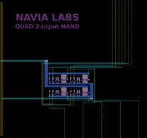
| 005 | 74HCT00 Quad 2-Input NAND (3.3 V) | Vipul Sharma · repository @engrvip123 | 1 × 2 | Analog and mixed-signal | 0 | |
| 007 | TT GF180mcuD Analog Factory Test | Sylvain Munaut · repository @smunaut | 1 × 2 | Test structures | 0 | |
| 033 | Simple Signal Generator | Matt Venn · repository @mattvenn | 1 × 2 | Other digital | 1,704 | 15k |
| 035 | GF R2R DAC | Matt Venn · repository @mattvenn | 1 × 2 | Analog and mixed-signal | 284 | 2k |
| 037 | algofoogle analog stuff | algofoogle (Anton Maurovic) · repository @algofoogle | 1 × 2 | Analog and mixed-signal | 695 | 6k |
| 038 | Hardware Entropy Explorer: UART/SPI TRNG and PUF | gojimmypi · repository @gojimmypi | 1 × 2 | Security | 3,281 | 28k |
| 039 | MoM capacitor | htfab · repository @htfab | 1 × 2 | Analog and mixed-signal | 0 | |
| 099 | Until heat death do us part | Julia Desmazes · repository @Essenceia | 2 × 2 | Communications | 3,961 | 17k |
| 101 | TT GF180mcuD Testbuffer | Christoph Weiser · repository @christoph-weiser | 1 × 2 | Analog and mixed-signal | 0 | |
| 102 | Tiny FABulous FPGA | Leo Moser · repository @mole99 | 4 × 4 | FPGA | 19,232 | 18k |
| 103 | tnt's recreation of a 555 on GF180mcu | Sylvain Munaut · repository @smunaut | 1 × 2 | Analog and mixed-signal | 0 | |
| 199 | TinyQV RISC-V SoC | Michael Bell · repository @MichaelBell | 4 × 2 | RISC-V and CPUs | 12,513 | 26k |
| 256 | 256x8 SRAM | Julia Desmazes · repository @Essenceia | 1 × 2 | Other digital | 96 | 1k |
| 258 | Abad2048 | Alexander Co Abad · repository @alexandercoabad | 1 × 2 | FPGA | 2,452 | 21k |
| 260 | GF BGR | Rahul Bhagwat · repository @bhagwat-rahul | 1 × 2 | Analog and mixed-signal | 0 | |
| 262 | Quadrature VCO | Sylvain Munaut · repository @smunaut | 1 × 2 | Analog and mixed-signal | 0 | |
| 288 | Philippine flag waving | Alexander Co Abad · repository @alexandercoabad | 1 × 2 | Other digital | 2,028 | 18k |
| 290 | Analog 4 bit Current DAC | Kiterai · repository @Kiterai | 1 × 2 | Analog and mixed-signal | 0 | |
| 292 | 3.3V Folded Cascode OTA | Pranay Arvind Patil and Nithin Purushothama · repository @chennakeshavadasa | 1 × 2 | Analog and mixed-signal | 0 | |
| 294 | Oscillating Bones | Uri Shaked · repository @urish | 1 × 2 | Other digital | 16 | <1k |
| 356 | 2048 sliding tile puzzle game (VGA) | Uri Shaked · repository @urish | 3 × 2 | Games | 6,736 | 19k |
| 358 | Hardware Entropy Explorer: UART/SPI TRNG and PUF (Analog) | gojimmypi · repository @gojimmypi | 1 × 2 | Security | 3,048 | 26k |
| 359 | Tiny FABulous FPGA (3.3V version) | Leo Moser · repository @mole99 | 4 × 4 | FPGA | 25,184 | 24k |
| 448 | wafer.space Logo VGA Screensaver | Uri Shaked | 1 × 2 | Art and logos | 2,228 | 19k |
| 450 | USB CDC (Serial) Device | Uri Shaked · repository @urish | 1 × 2 | Communications | 3,155 | 27k |
| 452 | PolyWave | Riccardo Pellegrini · repository @ODGrip | 1 × 2 | Other digital | 1,985 | 18k |
| 454 | MCML VCO | Namibj · repository @namibj | 1 × 2 | Analog and mixed-signal | 0 | |
| 518 | KianV uLinux SoC | Hirosh Dabui | 4 × 4 | RISC-V and CPUs | 20,266 | 19k |
| 519 | Simon Says memory game | Uri Shaked · repository @urish | 1 × 1 | Games | 1,301 | 23k |
Swipe the table sideways for more columns.
Designs that grew
Some designs on this chip have been made many times, on earlier and later Tiny Tapeout chips, and several now have a whole die of their own on a wafer.space run. The ringed marker is this chip.
56C6 One-hot FABulous FPGA
Caravel chip wafer.space Run 1 · Dec 2025
MOLE FABulous FPGA
1 × 1 slot Tiny Tapeout IHP 26a · Mar 2026
Tiny FABulous FPGA
8 × 4 tiles Tiny Tapeout SKY 26a · May 2026
Tiny FABulous FPGA
8 × 4 tiles Tiny Tapeout SKY 26b · May 2026
Tiny FABulous FPGA
8 × 4 tiles Tiny Tapeout GF 0.3 · Jun 2026
2 projects
4 × 4 tiles wafer.space Run 2 · Jul 2026
MOLE FABulous FPGA
1 × 1 slot Tiny Tapeout SKY 26c · Sep 2026
Tiny FABulous FPGA
8 × 4 tiles Tiny Tapeout IHP 26b · Sep 2026
Tiny FABulous FPGA
6 × 4 tiles
TinyQV RISC-V SoC
2 × 2 tiles Tiny Tapeout IHP 0.2 · Nov 2024
TinyQV RISC-V SoC
2 × 2 tiles Tiny Tapeout IHP 25a · Mar 2025
TinyQV RISC-V SoC
3 × 2 tiles Tiny Tapeout IHP 25b · Sep 2025
TinyQV - Crowdsourced RISC-V SoC
5 × 4 tiles Tiny Tapeout SKY 25a · Sep 2025
2 projects
8 × 4 tiles, 4 × 4 tiles Tiny Tapeout SKY 25b · Nov 2025
TinyQV RISC-V SoC
3 × 2 tiles Tiny Tapeout GF 0.1 · Nov 2025
TinyQV RISC-V SoC
in a shared block Tiny Tapeout GF 0.2 · Nov 2025
TinyQV RISC-V SoC
3 × 4 tiles wafer.space Run 1 · Dec 2025
3 dies
TQVA ½ × ½ slot, TQVB ½ × 1 slot, TQVC 1 × ½ slot Tiny Tapeout GF 0.3 · Jun 2026
TinyQV RISC-V SoC
4 × 2 tiles wafer.space Run 2 · Jul 2026
4 dies
TQVA ½ × ½ slot, TQVC 1 × ½ slot, TQVD ½ × ½ slot, TQVE ½ × ½ slot
KianV uLinux SoC
8 × 2 tiles Tiny Tapeout 6 · Apr 2024
KianV uLinux SoC
8 × 2 tiles Tiny Tapeout 7 · Jun 2024
KianV RISC-V RV32E Baremetal SoC
3 × 2 tiles Tiny Tapeout IHP 0.2 · Nov 2024
KianV RISC-V RV32E Baremetal SoC
4 × 2 tiles Tiny Tapeout GF 0.1 · Nov 2025
KianV uLinux SoC
in a shared block Tiny Tapeout GF 0.2 · Nov 2025
KianV uLinux SoC
4 × 4 tiles wafer.space Run 1 · Dec 2025
KIAN KianV: A 32-bit RISC-V Linux SoC taped out on GF180MCU
1 × 1 slot Tiny Tapeout IHP 26a · Mar 2026
KianV SV32 TT Linux SoC
8 × 4 tiles Tiny Tapeout GF 0.3 · Jun 2026
KianV uLinux SoC
4 × 4 tiles wafer.space Run 2 · Jul 2026
KIAN KianV: A 32-bit RISC-V Linux SoC taped out on GF180MCU Run 2
1 × 1 slot
Tiny Tapeout tile
Google shuttle
wafer.space die
this chip
Each marker is one version of the design: hover over it or focus it for details, and select it to open its
page. On a phone, the table below lists every one.
As a table
Analog and mixed-signal 11

Other digital 6
FPGA 3
Security 2
Test structures 2
Games 2
RISC-V and CPUs 2
Communications 2
Art and logos 1
Retro computing 1
Die T0P3 on wafer.space Run 2
The die as a whole, measured like every other design on its run: its size, pads, process features, density, precheck and photographs. See every design on wafer.space Run 2
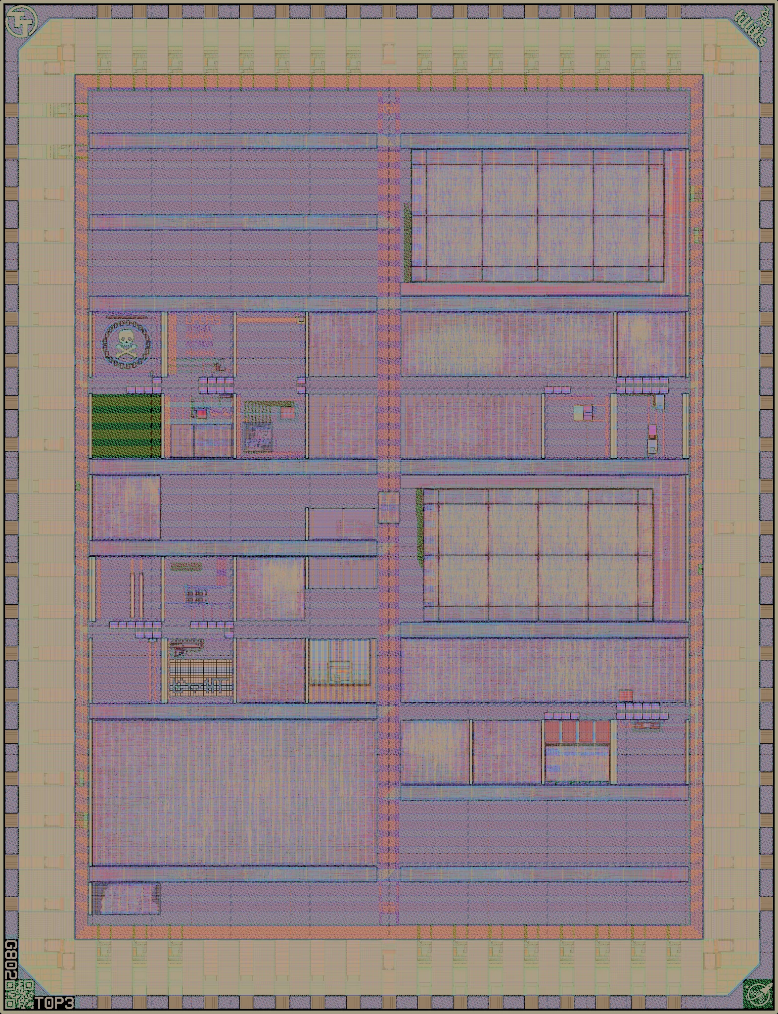
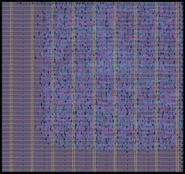
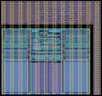
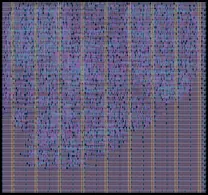
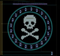
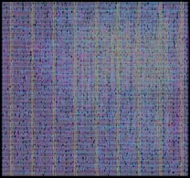
Rendered from the layout at 2.5 µm per pixel. Layers: NwellDiffusionPolysiliconMetal 1Metal 2Metal 3Metal 4Metal 5Top metalPad openings
Logic density
| Inside the core logic cells per mm² | 9k
(12% of buffer maximum) over the 12.90 mm² core: what the design itself packed |
|---|---|
| Inside the seal ring logic cells per mm² | 6k
over all 19.65 mm² of the slot, pad ring included |
| Densest mm² logic cells per mm² | 25k (32% of buffer maximum) |
| Core covered by logic | 27% |
| Transistor density transistors per mm² | 154k average, 328k in the mm² with the most logic cells |
Every figure here is measured from the public layout, the same way for every design on the run: see data and method, and how its designs used the process.
Experimental Tiny Tapeout shuttle with Analog design support
| Die | 3.93 × 5.12 mm (20.1 mm²) |
|---|---|
| Core area | 12.90 mm² inside the pad ring
the project template's, 442 µm in from each edge |
| Inside the seal ring | 19.65 mm² (the die less its 26 µm seal ring) |
| Placements | 1 on the reticle, in slot D5 |
| Bond pads | 74 |
| Transistors | 1,981,726 |
| Logic cells | 118,911 + 216,633 filler and tap cells |
| Libraries | 7t-5V (94k), AS 7t-3.3V (25k) |
| SRAM | 1 macro, 2,048 bits |
Submission
| Licence | Apache-2.0 declared
Repository: Apache-2.0 in LICENSE — agrees |
|---|---|
| How it was checked | Commit and PDK pinThe licence and template were read from the repository at commit 16c30128215e. |
| Chip-on-board | Not selected at submission |
| Precheck | Passed
the check it was accepted on, 2026-07-04
Passed latest re-run, 2026-08-02, gf180mcu-precheck 1.7.3 step results and logs |
Process features
Which parts of the GF180MCU process this design uses: its transistor voltages and where they come from, its gate oxides, and any devices drawn by hand outside the standard cells, SRAM and pads.
| 3.3 V | AS 7t-3.3V standard cells, ocd SRAM, 14,805 custom transistors |
|---|---|
| 5 V | 7t-5V standard cells, 4,426 custom transistors |
| 6 V | 80 custom transistors |
| Gate oxides | Thin (3.3 V) and thick (5 V/6 V) in the design itself |
| MOS capacitors | 12 (1,200 µm²) |
| High-resistance poly resistors | 511 (26,587 µm²) |
| Unsalicided poly resistors | 12 (102 µm²) |
| Deep N-well | 9 (1,253 µm²) |
| Bipolar transistors | 9 (225 µm²) |
| I/O library | gf180mcu_ocd_io (1140 cells) |
Where the area went
How this design's area splits between logic cells, SRAM, filler and tap cells, other and pad ring.
- Logic cells 3.47 mm² (17%)
- SRAM 0.07 mm² (<1%)
- Filler and tap cells 2.95 mm² (15%)
- Other 6.41 mm² (32%)
- Pad ring 7.22 mm² (36%)
Most used cells
The ten standard cells this design uses most.
| Cell | Library | Instances | What it does |
|---|---|---|---|
| nand2_1 | 7t-5V | 7,751 | 2-input NAND gate |
| mux2_2 | AS 7t-3.3V | 6,796 | 2-input multiplexer (2x drive) |
| buf_1 | 7t-5V | 6,487 | Buffer |
| nor2_1 | 7t-5V | 6,134 | 2-input NOR gate |
| dlxfp_2 | AS 7t-3.3V | 5,504 | Latch (level-sensitive, 2x drive) |
| latq_1 | 7t-5V | 5,504 | Latch (level-sensitive) |
| aoi21_1 | 7t-5V | 5,099 | AND-OR-Invert compound gate |
| dffq_1 | 7t-5V | 5,096 | D flip-flop (1 bit storage) |
| buff_2 | AS 7t-3.3V | 4,980 | Buffer (2x drive) |
| oai21_1 | 7t-5V | 3,545 | OR-AND-Invert compound gate |
Logic density map
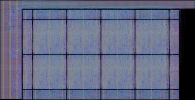
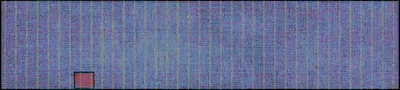
Logic cells per mm² in each square millimetre of the die. Hatched outlines are SRAM macros; the red outline is the densest mm² that avoids them (25k logic cells per mm²), found by sliding a 1 mm square over the die in 0.1 mm steps, so it can straddle the fixed squares and find more than any one of them. Squares at the edges are partial, so they read low.
SRAM macros
The ready-made memory blocks this design uses.
| Macro | Count | Bits each |
|---|---|---|
| gf180mcu_ocd_ip_sram__sram256x8m8wm1 | 1 | 2,048 |
Precheck
Before a design is made, the wafer.space platform checks it against the foundry's design rules. T0P3 was accepted on this check, and has been checked again since with newer rules.
All 16 steps passed, with 0 KLayout DRC errors, on 2026-07-04.
Every step, and the latest re-run
| Step | Accepted on check 336, 2026-07-04, initial | Latest re-run check 741, 2026-08-02, drc_update, gf180mcu-precheck 1.7.3 PDK open_pdks 1.0.604, LibreLane 5fe3db1 |
|---|---|---|
| KLayout.ReadLayout | passed | passed |
| KLayout.CheckTopLevel | passed | passed |
| KLayout.CheckSize | passed | passed |
| KLayout.GenerateID | passed | passed |
| KLayout.Render | passed | passed |
| KLayout.Density | passed | passed |
| Checker.KLayoutDensity | passed | passed |
| KLayout.ZeroAreaPolygons | passed | passed |
| Checker.KLayoutZeroAreaPolygons | passed | passed |
| KLayout.Antenna | passed | passed |
| Checker.KLayoutAntenna | passed | passed |
| Magic.DRC | passed | passed |
| Checker.MagicDRC | advisory warning | advisory warning |
| KLayout.DRC | passed | passed |
| Checker.KLayoutDRC | passed | passed |
| KLayout.WriteLayout | passed | passed |
| KLayout DRC errors | 0 | 0 |
| Magic DRC errors (advisory) | 2,268 | 2,268 |
| Files | steps · log (gzip) | steps · log (gzip) |
The steps of the gf180mcu-precheck LibreLane flow, as run by platform.wafer.space. The design was accepted on the newest finished check before it was submitted; later re-runs check the same file with updated rules. KLayout DRC is the sign-off check. Magic DRC is advisory: its count does not stop a design. In the logs, Magic's "Error while reading cell" lines about fill cells are messages from its reader, not check failures.
Data and method
Everything on this page is measured from the public layout; the dates come from the published schedules.
- Logic cells are standard cell instances, excluding fillers, taps, antenna diodes and tie cells.
- Transistors are places where gate polysilicon crosses diffusion, not counting dummy fill.
- Core area is the whole project.
- Bond pads are the pad openings in the pad ring, or in a second ring of pads inside it for chip-on-board bonding; probe pads are the others, next to the blocks they test. Letters and logos on the pad layer are not pads.
- Theoretical maximum tiles one cell at its placement boundary with no routing.
- Densest 0.1 mm square is the best 0.1 mm square anywhere in each die, sliding in 20 µm steps and avoiding SRAM, given per mm².
The full written analysis is the density report. The measurements behind it:
- reticle_analysis.csv
- reticle_analysis_cells.csv
- reticle_analysis_content.csv
- reticle_analysis_features.csv
- reticle_analysis_grid.csv
- reticle_analysis_library.csv
- reticle_analysis_macros.csv
- reticle_analysis_map.csv
- reticle_analysis_meta.json
- reticle_analysis_metal.csv
- reticle_analysis_provenance.csv
- reticle_analysis_slot_areas.csv
- reticle_analysis_slot_macros.csv
- reticle_analysis_sram_rects.csv
- reticle_analysis_usage.csv
- reticle_analysis_windows.csv
- reticle_density_report.md
Generated by ws-run-reports from layout/T0P3.oas (md5 bfd37b3547ee338c21a9689a031bbb0c).
What is Tiny Tapeout?
Tiny Tapeout is the quickest and cheapest way to get your own design made on a real chip.
Many designs share one Tiny Tapeout chip. Each project gets one or more small tiles, and a multiplexer on the chip connects the one you choose to the pins. Draw your first design in the browser with no experience by following the digital design guide, or write it in Verilog or another HDL; Tiny Tapeout's templates build and check it on GitHub. The chip comes on a demo board that selects your design and drives it.
Tiny Tapeout also runs workshops and supports teaching in universities and schools. Browse every Tiny Tapeout chip and the projects proven in silicon, or read the Tiny Tapeout FAQ.
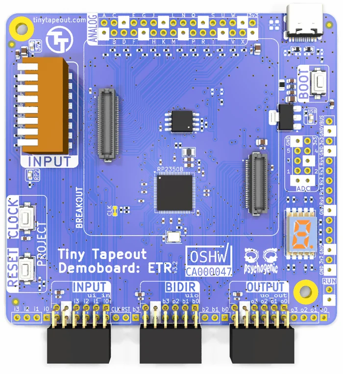

Tiny Tapeout and wafer.space are independent companies that work together (announcement). Tiny Tapeout runs its own shuttles: it takes the projects, builds the die, and sells and supports the chips and boards. wafer.space has the dies manufactured on its GF180MCU runs, and these pages are wafer.space's measurements of them. For anything about a Tiny Tapeout project, chip or order, contact Tiny Tapeout.