Tiny Tapeout GF 0.1Made on a GlobalFoundries private MPW run
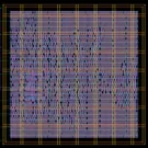
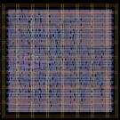
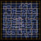
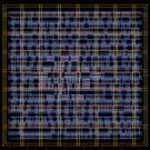
Tiny Tapeout's first, experimental GF180MCU chip. Instead of tiles, its 24 projects, all from earlier Tiny Tapeout chips, were built together into one shared block. Eight small blocks beside it test standard cell libraries from GlobalFoundries, Avalon Semiconductors and OSU on this process.
What was built
The chip as a whole: what its projects add up to.
24
Projects
in one shared block
8
Cell tests
and a pad test
800k
Transistors
across the unique designs
72k
Logic cells
gates and flip-flops
Counted inside the blocks: the shared project block (with its multiplexer), the cell tests and the pad test buffer. The pads and the fill are left out.
Get this chip, or make your own
Tiny Tapeout puts many small designs on one chip. Start with a tile, then come back with a whole die.
Get a Tiny Tapeout chip
This test chip was not sold. The Tiny Tapeout chips made since come on a board you can plug in and try.
Buy a chip and boardPut your design on the next one
Tiny Tapeout GF 26c and 26d take projects until 7 December 2026, to be made on wafer.space Run 3.
Submit a projectMake a whole chip of your own
When a design outgrows a few tiles, it can have a die to itself on wafer.space Run 3: orders close 9 December 2026.
Reserve a slotThe die
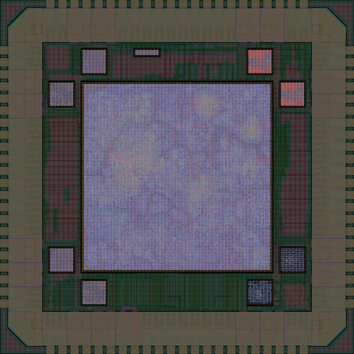
Every design rendered from the layout at the same scale and placed where it sits on the 2.9 × 2.9 mm die. Point at a block to see its name, and select it for its details.Every block is listed further down.
Shuttle status
- 24 November 2025 Tiny Tapeout GF 0.1 tapeout release Tiny Tapeout publishes the die's final layout (v23) for a GlobalFoundries private MPW run
- Today, 24 October 2026
Missed this one? Tiny Tapeout GF 26c and 26d take projects until 7 December 2026: submit a project.
Tiny Tapeout has not published dates after tapeout for this test chip.
How people used their silicon
Where the area of 10 blocks (3 mm² of silicon) actually went
- Logic cells 65% — gates and flip-flops doing the design's actual work
- Filler and tap cells 25% — inserted by the tools to keep rows continuous and wells tied
- Other 10% — routing channels, analog and custom layout, power grid and empty space
Standard cell libraries
The ready-made gate libraries the designs were built from: how many tracks tall each cell is, and the voltage it runs at.
| Standard cell library | Logic cells | Share |
|---|---|---|
| 7t-5V gf180mcu_fd_sc_mcu7t5v0 | 64k | 89% |
| AS 7t-3.3V gf180mcu_as_sc_mcu7t3v3 | 2k | 3% |
| OSU 12t-3.3V gf180mcu_osu_sc_gp12t3v3 | 1k | 2% |
| OSU 9t-3.3V gf180mcu_osu_sc_gp9t3v3 | 1k | 2% |
| 7t-5V as 3.3V gf180mcu_hfd_sc_mcu7t5v0 | 1k | 1% |
| 9t-5V gf180mcu_fd_sc_mcu9t5v0 | 1k | 1% |
| 9t-5V as 3.3V gf180mcu_hfd_sc_mcu9t5v0 | 1k | 1% |
Area budget of every design
Each bar is one block, split the same way as above. Sorted by how much of the block is logic.
What fits on 1 mm² of GF180MCU silicon?
Theoretical maximum against what designers achieved
The maximum packs one cell type edge to edge with no room for wiring. Real designs need the wiring. Each box gives the most of a cell that fits with any GF180MCU library, then with the libraries this chip used.
~114k
Inverters per mm²
GF180MCU maximum,
with
AS 7t-3.3V
inv_2
With this chip's libraries:
AS 7t-3.3V: 114k inv_2
7t-5V as 3.3V: 114k inv_1
9t-5V as 3.3V: 89k inv_1
~91k
NAND gates per mm²
GF180MCU maximum,
with
7t-5V
nand2_1
With this chip's libraries:
AS 7t-3.3V: 65k nand2_2
OSU 12t-3.3V: 39k nand2_1
OSU 9t-3.3V: 51k nand2_1
7t-5V as 3.3V: 91k nand2_1
9t-5V as 3.3V: 71k nand2_1
~76k
Buffers per mm²
GF180MCU maximum,
with
AS 7t-3.3V
buff_2
With this chip's libraries:
AS 7t-3.3V: 76k buff_2
7t-5V as 3.3V: 76k buf_1
9t-5V as 3.3V: 59k buf_1
~17k
Flip-flops per mm²
GF180MCU maximum,
with
AS 7t-3.3V
dfxtp_2
With this chip's libraries:
AS 7t-3.3V: 17k dfxtp_2
OSU 12t-3.3V: 9k dff_1
OSU 9t-3.3V: 11k dff_1
7t-5V as 3.3V: 16k dffq_1
9t-5V as 3.3V: 13k dffq_1
25k
Best core average
logic cells/mm² of core — 32% of the buffer maximum
48k
Densest 0.1 mm square
logic cells per mm² — 63% of the buffer maximum
20k
Typical block
median logic cells/mm² of core across 9 digital blocks (1,000 or more logic cells)
29% of the core covered by logic cells
Percentages compare with the buffer maximum for each design's own library: buffers are among the smallest and most common logic cells, so a design made only of buffers, packed edge to edge with no wiring, would reach 100%.
Sizing your own design
This chip had no tiles: its projects shared one block, so it cannot tell you what a tile holds. For tile sizes, see the later chips, from Tiny Tapeout GF 0.2 on.
Logic density of every digital design
A digital block here is one with 1,000 or more logic cells. Solid bar: average over the core. Outlined bar: the densest 0.1 mm square outside SRAM, per mm² (a dash where memory covers most of the design). The scale ends at the buffer theoretical maximum (76k cells/mm²). The numbers are core / densest, in logic cells per mm².
Every digital block's densities as a table
| Project | Tiles | Library | Logic cells | Inside core per mm² |
Densest 0.1 mm square per mm² |
Core covered | Core mm² |
|---|---|---|---|---|---|---|---|
| The 24 Tiny Tapeout projects MAIN | 1.6 × 1.6 mm | 7t-5V | 63,000 | 24,609 | 43,400 | 72% | 2.56* |
| Cell test: OSU 12-track 3.3 V cells CEL5 | 0.225 × 0.225 mm | OSU 12t-3.3V | 1,082 | 20,454 | 29,800 | 41% | 0.05* |
| Cell test: OSU 9-track 3.3 V cells CEL4 | 0.225 × 0.225 mm | OSU 9t-3.3V | 1,081 | 20,435 | 32,400 | 32% | 0.05* |
| Cell test: AS 7-track 3.3 V cells CEL6 | 0.225 × 0.225 mm | AS 7t-3.3V | 1,080 | 20,416 | 47,900 | 20% | 0.05* |
| Cell test: AS 7-track 3.3 V cells, second copy CEL7 | 0.225 × 0.225 mm | AS 7t-3.3V | 1,080 | 20,416 | 47,900 | 20% | 0.05* |
| Cell test: GF 7-track 5 V cells CEL0 | 0.225 × 0.225 mm | 7t-5V | 1,074 | 20,302 | 45,100 | 29% | 0.05* |
| Cell test: GF 7-track cells as 3.3 V transistors CEL2 | 0.225 × 0.225 mm | 7t-5V as 3.3V | 1,074 | 20,302 | 45,100 | 29% | 0.05* |
| Cell test: GF 9-track 5 V cells CEL1 | 0.225 × 0.225 mm | 9t-5V | 1,071 | 20,246 | 44,300 | 29% | 0.05* |
| Cell test: GF 9-track cells as 3.3 V transistors CEL3 | 0.225 × 0.225 mm | 9t-5V as 3.3V | 1,071 | 20,246 | 44,300 | 29% | 0.05* |
The projects
Every project on this chip: an index, then grouped by what it does. Select one for its layout, its measurements and any die photographs.
Designs that grew
Some designs on this chip have been made many times, on earlier and later Tiny Tapeout chips, and several now have a whole die of their own on a wafer.space run. The ringed marker is this chip.
TinyQV RISC-V SoC
2 × 2 tiles Tiny Tapeout IHP 0.2 · Nov 2024
TinyQV RISC-V SoC
2 × 2 tiles Tiny Tapeout IHP 25a · Mar 2025
TinyQV RISC-V SoC
3 × 2 tiles Tiny Tapeout IHP 25b · Sep 2025
TinyQV - Crowdsourced RISC-V SoC
5 × 4 tiles Tiny Tapeout SKY 25a · Sep 2025
2 projects
8 × 4 tiles, 4 × 4 tiles Tiny Tapeout SKY 25b · Nov 2025
TinyQV RISC-V SoC
3 × 2 tiles Tiny Tapeout GF 0.1 · Nov 2025
TinyQV RISC-V SoC
in a shared block Tiny Tapeout GF 0.2 · Nov 2025
TinyQV RISC-V SoC
3 × 4 tiles wafer.space Run 1 · Dec 2025
3 dies
TQVA ½ × ½ slot, TQVB ½ × 1 slot, TQVC 1 × ½ slot Tiny Tapeout GF 0.3 · Jun 2026
TinyQV RISC-V SoC
4 × 2 tiles wafer.space Run 2 · Jul 2026
4 dies
TQVA ½ × ½ slot, TQVC 1 × ½ slot, TQVD ½ × ½ slot, TQVE ½ × ½ slot
KianV uLinux SoC
8 × 2 tiles Tiny Tapeout 6 · Apr 2024
KianV uLinux SoC
8 × 2 tiles Tiny Tapeout 7 · Jun 2024
KianV RISC-V RV32E Baremetal SoC
3 × 2 tiles Tiny Tapeout IHP 0.2 · Nov 2024
KianV RISC-V RV32E Baremetal SoC
4 × 2 tiles Tiny Tapeout GF 0.1 · Nov 2025
KianV uLinux SoC
in a shared block Tiny Tapeout GF 0.2 · Nov 2025
KianV uLinux SoC
4 × 4 tiles wafer.space Run 1 · Dec 2025
KIAN KianV: A 32-bit RISC-V Linux SoC taped out on GF180MCU
1 × 1 slot Tiny Tapeout IHP 26a · Mar 2026
KianV SV32 TT Linux SoC
8 × 4 tiles Tiny Tapeout GF 0.3 · Jun 2026
KianV uLinux SoC
4 × 4 tiles wafer.space Run 2 · Jul 2026
KIAN KianV: A 32-bit RISC-V Linux SoC taped out on GF180MCU Run 2
1 × 1 slot
raybox-zero
4 × 2 tiles Tiny Tapeout 7 · Jun 2024
raybox-zero TT07 edition
6 × 2 tiles Tiny Tapeout IHP 0.2 · Nov 2024
raybox-zero TTIHP0p2 edition
4 × 2 tiles Tiny Tapeout GF 0.1 · Nov 2025
raybox-zero TT07 edition
in a shared block Tiny Tapeout GF 0.2 · Nov 2025
raybox-zero TTGF0p2 edition
3 × 4 tiles Tiny Tapeout IHP 0.4 · Mar 2026
raybox-zero TTIHP0p4 edition
6 × 2 tiles wafer.space Run 2 · Jul 2026
AMM1 raybox-zero wafer.space run 2 half height
1 × ½ slot
Tiny Tapeout tile
Google shuttle
wafer.space die
this chip
Each marker is one version of the design: hover over it or focus it for details, and select it to open its
page. On a phone, the table below lists every one.
As a table
The 24 projects
On this first Tiny Tapeout GF180MCU chip the projects did not get tiles of their own: all 24 were synthesised and placed together in one block, behind the multiplexer that selects one at a time. So each project's size here is counted from that block's netlist, cell by cell. Original tiles is the project's size on the Tiny Tapeout chip it first came from.
| Address | Project | Author | Original tiles | Logic cells | Flip-flops | Share of the block |
|---|---|---|---|---|---|---|
| 000 | Chip ROM | Uri Shaked | 1×1 | in the shared logic | ||
| 001 | TinyTapeout Factory Test | Tiny Tapeout | 1×1 | 70 | 9 | 0.1% |
| 002 | Pad Test | htfab | 1×1 | 218 | 27 | 0.3% |
| 003 | Simon Says memory game | Uri Shaked · repository @urish | 1×1 | 1,242 | 194 | 2.0% |
| 004 | VGA clock | Matt Venn · repository @mattvenn | 1×1 | 847 | 146 | 1.3% |
| 005 | 7-Seg 'Tiny Tapeout' Display | J. Rosenthal & htfab · repository @htfab | 1×1 | 55 | 4 | 0.1% |
| 006 | Neptune guitar tuner (proportional window, version b, debug output on bidir pins, larger set of frequencies) | Pat Deegan · repository @psychogenic | 1×1 | 868 | 136 | 1.4% |
| 007 | RGB Mixer demo | Matt Venn · repository @mattvenn | 1×1 | 551 | 111 | 0.9% |
| 008 | MULDIV unit (4-bit signed/unsigned) | Darryl Miles · repository @dlmiles | 1×1 | in the shared logic | ||
| 009 | One Sprite Pony | Leo Moser · repository @mole99 | 1×1 | 1,190 | 255 | 1.9% |
| 010 | VGA Experiments | Tom Keddie · repository @TomKeddie | 1×1 | 950 | 95 | 1.5% |
| 011 | Super Mario Tune on A Piezo Speaker | Milosch Meriac · repository @meriac | 1×1 | 442 | 52 | 0.7% |
| 012 | ROTFPGA v2 | htfab · repository @htfab | 1×1 | 2,179 | 64 | 3.5% |
| 013 | Character Selector | Dakota W Winslow · repository @dakotawinslow | 1×1 | 141 | 3 | 0.2% |
| 014 | Flappy VGA | Daniel Robinson · repository @Cutout1 | 1×1 | 683 | 82 | 1.1% |
| 015 | Classic 8-bit era Programmable Sound Generator AY-3-8913 | ReJ aka Renaldas Zioma · repository @rejunity | 1×1 | 1,351 | 219 | 2.1% |
| 016 | UART uwuifier | Anish Singhani · repository @asinghani | 1×1 | 634 | 135 | 1.0% |
| 017 | USB CDC (Serial) | Uri Shaked | 1×2 | 2,622 | 383 | 4.2% |
| 018 | Tiny Breakout | Robbert-Jan de Jager · repository @robojan | 1×2 | 1,961 | 400 | 3.1% |
| 019 | TinyQV Risc-V SoC | Michael Bell · repository @MichaelBell | 2×2 | 5,477 | 1,036 | 8.7% |
| 020 | VGA Dino Game | Anish Singhani · repository @asinghani | 2×2 | 3,143 | 263 | 5.0% |
| 021 | No Time for Squares | Tommy Thorn · repository @tommythorn | 3×2 | 6,459 | 651 | 10.3% |
| 022 | raybox-zero TT07 edition | algofoogle (Anton Maurovic) · repository @algofoogle | 6×2 | 12,093 | 1,357 | 19.2% |
| 023 | KianV uLinux SoC | Hirosh Dabui · repository @splinedrive | 8×2 | 19,265 | 2,563 | 30.6% |
| The multiplexer and controller, with Chip ROM and the MULDIV unit | 559 | 3 | 0.9% |
A cell belongs to the project its nets are named after, or to the one project of the cells it is wired to. Chip ROM and the MULDIV unit are purely combinational, so synthesis kept no names for their cells: they are counted with the shared multiplexer and controller. The 63,000 logic cells in all are exactly the block's logic cells as measured from the layout.
The blocks
The die's own blocks, each measured like a design: the shared block that holds the projects, eight standard cell tests and the pad test buffer.
Test structures 9
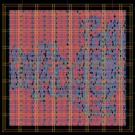
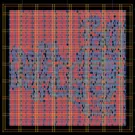
Shared project block 1
Data and method
The die and its blocks are measured from the public layout; each project's share of the shared block is counted from that block's netlist.
- Logic cells are standard cell instances, excluding fillers, taps, antenna diodes and tie cells.
- Transistors are places where gate polysilicon crosses diffusion, not counting dummy fill.
- Core area is the whole block.
- Bond pads are the pad openings in the pad ring, or in a second ring of pads inside it for chip-on-board bonding; probe pads are the others, next to the blocks they test. Letters and logos on the pad layer are not pads.
- Theoretical maximum tiles one cell at its placement boundary with no routing.
- Densest 0.1 mm square is the best 0.1 mm square anywhere in each die, sliding in 20 µm steps and avoiding SRAM, given per mm².
The full written analysis is the density report. The measurements behind it:
- reticle_analysis.csv
- reticle_analysis_cells.csv
- reticle_analysis_content.csv
- reticle_analysis_features.csv
- reticle_analysis_grid.csv
- reticle_analysis_library.csv
- reticle_analysis_macros.csv
- reticle_analysis_map.csv
- reticle_analysis_meta.json
- reticle_analysis_metal.csv
- reticle_analysis_provenance.csv
- reticle_analysis_slot_areas.csv
- reticle_analysis_slot_macros.csv
- reticle_analysis_sram_rects.csv
- reticle_analysis_usage.csv
- reticle_analysis_windows.csv
- reticle_density_report.md
Generated by ws-run-reports from layout/T0P1.oas (md5 1064ed9cfa033b91c1a45309a916fa83).
What is Tiny Tapeout?
Tiny Tapeout is the quickest and cheapest way to get your own design made on a real chip.
Many designs share one Tiny Tapeout chip. Each project gets one or more small tiles, and a multiplexer on the chip connects the one you choose to the pins. Draw your first design in the browser with no experience by following the digital design guide, or write it in Verilog or another HDL; Tiny Tapeout's templates build and check it on GitHub. The chip comes on a demo board that selects your design and drives it.
Tiny Tapeout also runs workshops and supports teaching in universities and schools. Browse every Tiny Tapeout chip and the projects proven in silicon, or read the Tiny Tapeout FAQ.
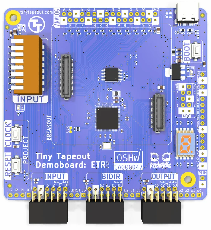

Tiny Tapeout and wafer.space are independent companies that work together (announcement). Tiny Tapeout runs its own shuttles: it takes the projects, builds the die, and sells and supports the chips and boards. wafer.space has the dies manufactured on its GF180MCU runs, and these pages are wafer.space's measurements of them. For anything about a Tiny Tapeout project, chip or order, contact Tiny Tapeout.