Google GF180MCU test shuttle (MPW‑18H1)Made on a private GlobalFoundries MPW run
4 public designs on one GF180MCU reticle
What was built
The run as a whole: what its designs add up to.
A private GF180MCU test shuttle on GlobalFoundries' MPW service, with four test designs. Each sat in the user area of the Caravel harness, which took 55% of every die for its management SoC, pads and wiring. They are measured here the same way as wafer.space's own runs, for comparison with a wafer.space die, where everything inside the pad ring is your design. The other Google shuttle measured here is GFMPW-0.
4
Public designs
filling all 4 slots
4
Open source
with a public repository
272k
Transistors
across the unique designs
8k
Logic cells
gates and flip-flops
4
Whole dies
every slot a whole die
Private designs on the reticle are not in the public layout and are not counted. Designs placed more than once are counted once.
Make a chip of your own
These designs were made free on one of Google's shuttles. The same GF180MCU process is open to anyone on wafer.space: start small with a Tiny Tapeout tile, or go straight to a whole die on the next wafer.space run.
Make a whole chip of your own
Book a die to itself on wafer.space Run 3: orders close 9 December 2026.
Reserve a slotOr start with a Tiny Tapeout tile
Tiny Tapeout GF 26c and 26d take projects until 7 December 2026, to be made on wafer.space Run 3.
Submit a projectGet a Tiny Tapeout chip
Every Tiny Tapeout chip comes on a board you can plug in, with all of its projects ready to try.
Buy a chip and boardThe reticle
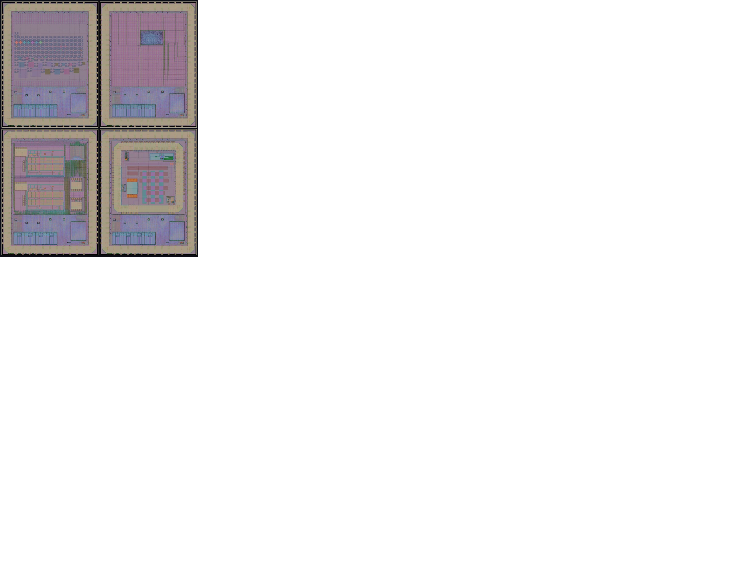
Every design rendered from the layout at the same scale and placed where it sits on the 8 × 10.4 mm reticle. It is drawn at the same scale as the 30 × 23.4 mm reticles of wafer.space Runs 1 and 2, so its dies can be compared with theirs. Point at a die to see its name, and select it for its details.Every die is listed further down.
Slots
How much of the reticle each design took: a 1 × 1 slot is a whole die of its own.
| 1 × 1 | 4 |
| Total | 4 |
|---|
Shuttle status
How this run went, from the call for designs to the finished chips.
- 1 February 2023 Tapeout flow set up Google adds the GF180MCU tapeout flow to the four projects' repositories
- 26 February – 3 March 2023 Designs submitted The designers' final layouts for GF submission
- about 3 March 2023 Tapeout Final Caravel dies written (2–3 March) for GlobalFoundries' private MPW run 18H1
- 20 December 2023 Final dies published Google publishes the final dies and the shuttle's list of projects
- 2024 Silicon results published Measured results of the OpenFASoC analog front-end (0004), in IEEE Solid-State Circuits Magazine
- June – July 2025 Die photographs John McMaster photographs dies 0001 and 0004 for Silicon Prawn
- Today, 24 October 2026
How people used their silicon
Where the area of 4 dies (80 mm² of silicon) actually went
- Logic cells <1% — gates and flip-flops doing the design's actual work
- Filler and tap cells 1% — inserted by the tools to keep rows continuous and wells tied
- Other 43% — routing channels, analog and custom layout, power grid and empty space
- Outside the user area 55% — the Caravel harness around the user's design: its management SoC, pads and wiring
What people built
The kinds of design on this run.
Test structures 2 Analog and mixed-signal 1 Other digital 1Standard cell libraries
The ready-made gate libraries the designs were built from: how many tracks tall each cell is, and the voltage it runs at.
| Standard cell library | Logic cells | Share |
|---|---|---|
| OSU 9t-3.3V gf180mcu_osu_sc_gp9t3v3 | 7k | 88% |
| 7t-5V gf180mcu_fd_sc_mcu7t5v0 | 1k | 12% |
Area budget of every design
Each bar is one die, split the same way as above. Sorted by how much of the die is logic.
Which parts of the process were used
Transistor voltages and optional devices across the 4 designs
Transistor voltages
A design counts for a voltage when its standard cells, SRAM or its own transistors use it. 5 V and 6 V transistors share the thick gate oxide; a marker layer in the layout tells them apart.
Optional devices drawn by designers
Not drawn by any design: Native transistors, 10 V LDMOS, MOS capacitors, Salicided poly resistors, Diffusion resistors, N-well resistors, Metal resistors, Well diodes, Bipolar transistors, Schottky diodes, Zener diodes, eFuses, One-time programmable memory, Inductors.
Only devices outside standard cells, SRAM macros and I/O pads count, since every die has those. A single test structure counts the same as a large block.
Gate oxides
| Transistors | Own design | With the pad ring | Which (own design) |
|---|---|---|---|
| 3.3 V and 5 V/6 V | 2 | 2 | Fitbit test IC 1, Analog front-end for sensor readout (OpenFASoC) |
| 3.3 V only | 1 | 1 | OSU 3.3V standard cell test (vlsiffra adder) |
| 5 V/6 V only | 0 | 0 |
3.3 V transistors have the thin gate oxide; 5 V and 6 V ones share the thick one. "Own design" counts the standard cells, SRAM and transistors the designer chose; "with the pad ring" adds the transistors of the I/O pad cells, measured in each design's pad ring. No transistors of their own: LibreSilicon Danube River test tile.
What fits on 1 mm² of GF180MCU silicon?
Theoretical maximum against what designers achieved
The maximum packs one cell type edge to edge with no room for wiring. Real designs need the wiring. Each box gives the most of a cell that fits with any GF180MCU library, then with the libraries this run used.
~76k
Buffers per mm²
GF180MCU maximum,
with
AS 7t-3.3V
buff_2
With this run's libraries:
OSU 9t-3.3V: 49k buf_1
~17k
Flip-flops per mm²
GF180MCU maximum,
with
AS 7t-3.3V
dfxtp_2
With this run's libraries:
OSU 9t-3.3V: 11k dff_1
This shuttle has only 1 die with 1,000 or more logic cells, too few for a best or typical figure. For densities across dozens of designs, see wafer.space Run 2.
Sizing your own design
With only 1 die of 1,000 or more logic cells, this shuttle cannot say what a slot typically holds. wafer.space Run 2's page sizes each slot from dozens of designs.
Logic density of every digital design
A digital die here is one with 1,000 or more logic cells. Solid bar: average over the core. Outlined bar: the densest mm² outside SRAM (a dash where memory covers most of the design). The scale ends at the buffer theoretical maximum (76k cells/mm²). The numbers are core / densest, in logic cells per mm².
Every digital die's densities as a table
| Design | Slot | Library | Logic cells | Inside core per mm² |
Densest mm² per mm² |
Core covered | Core mm² |
|---|---|---|---|---|---|---|---|
| OSU 3.3V standard cell test (vlsiffra adder) 0002 | 1 × 1 | OSU 9t-3.3V | 7,341 | 816 | 7,341 | 2% | 9.00 |
The projects
Every design on this run: an index, then grouped by what it does. Select one for its layout, its measurements and any die photographs.
Design index
All 4 public designs by their code, with the slot each took and how much logic it packs.
| Code | Design | Slot | What it is | Logic cells | Cells per mm² |
|---|---|---|---|---|---|
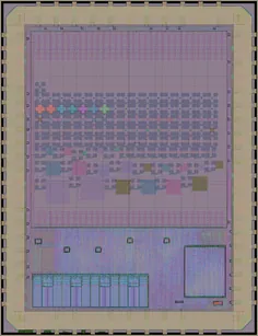
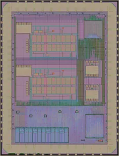
| 0001 | LibreSilicon Danube River test tile | 1 × 1 | Test structures | 0 | |
| 0002 | OSU 3.3V standard cell test (vlsiffra adder) | 1 × 1 | Other digital | 7,341 | 1k |
| 0003 | Fitbit test IC 1 | 1 × 1 | Test structures | 800 | <1k |
| 0004 | Analog front-end for sensor readout (OpenFASoC) | 1 × 1 | Analog and mixed-signal | 248 | <1k |
Swipe the table sideways for more columns.
Test structures 2
Analog and mixed-signal 1
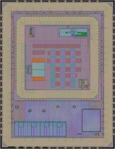
Other digital 1
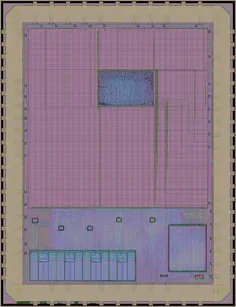
The real silicon
Optical micrographs of the fabricated dies © 2025 John McMaster, CC BY 4.0
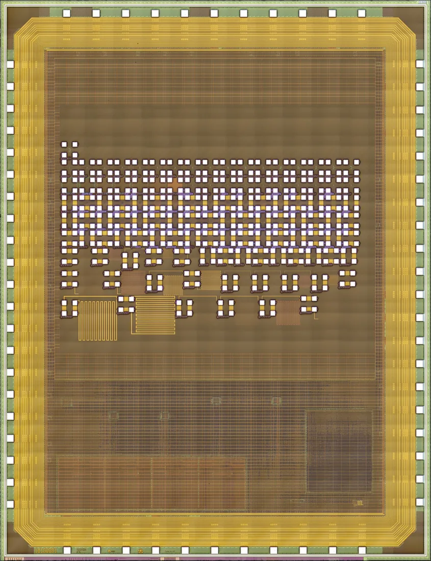
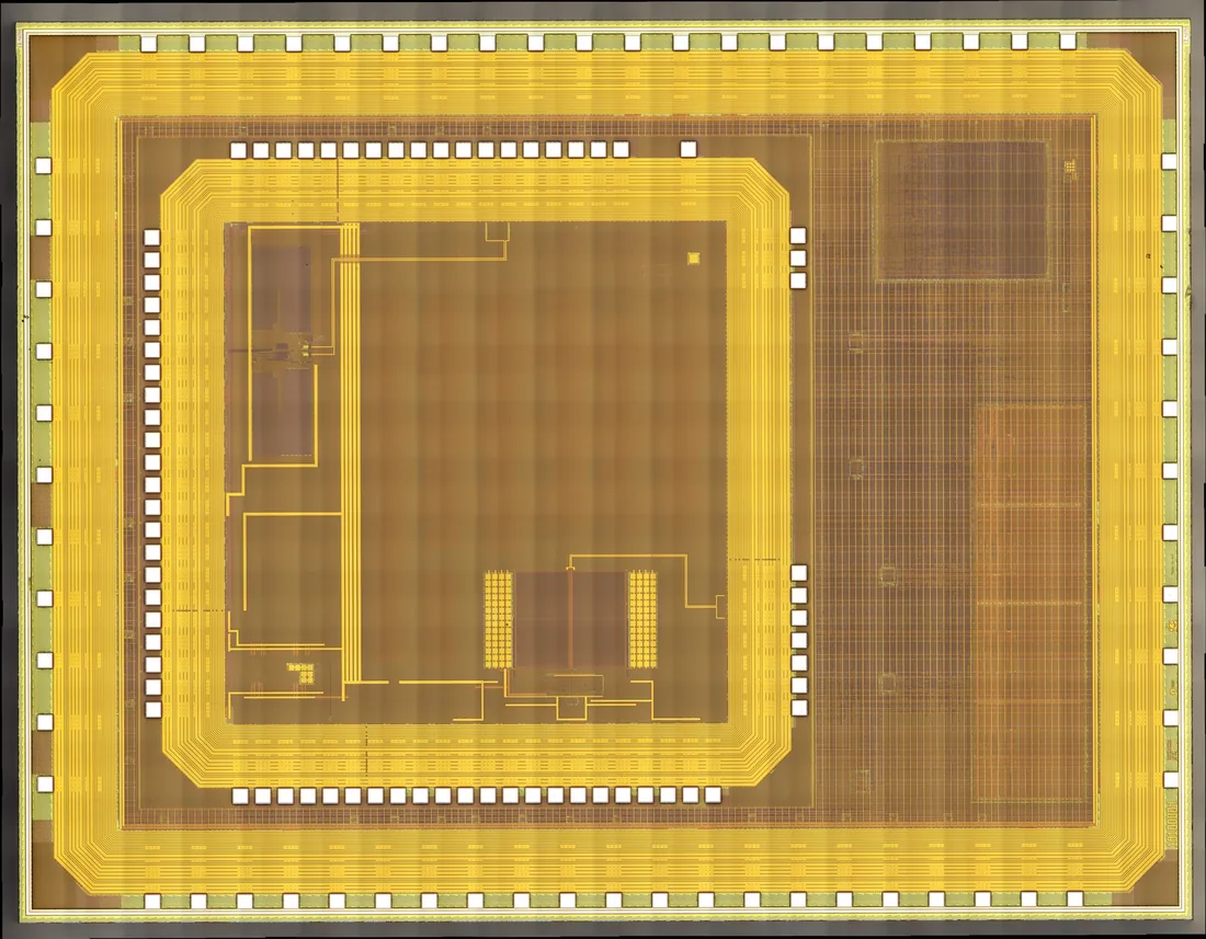
Microscope images © 2025 John McMaster, CC BY 4.0. Each project page links to a zoomable viewer of its die. The full-resolution images are online too.
Data and method
Everything on this page is measured from the public layout; the dates come from the shuttle repositories, the dies' GDS headers, the OpenFASoC paper and the Silicon Prawn photographs (no schedule was published for this private shuttle).
- Logic cells are standard cell instances, excluding fillers, taps, antenna diodes and tie cells.
- Transistors are places where gate polysilicon crosses diffusion, not counting dummy fill.
- Core area is the area of each die's user_project_wrapper cell.
- Excluded from the measurements: pad ring (gf180mcu_*_io__*); caravel harness (caravel_core, caravel_power_routing, chip_io, caravel_logo, caravel_motto, copyright_block, open_source, user_id_textblock); seal ring (sealring). Die sizes are measured on the whole die, and bond pads on the whole die apart from its seal ring.
- Bond pads are the pad openings in the pad ring, or in a second ring of pads inside it for chip-on-board bonding; probe pads are the others, next to the blocks they test. Letters and logos on the pad layer are not pads.
- Theoretical maximum tiles one cell at its placement boundary with no routing.
- Densest mm² is the best 1 mm square anywhere in each die, sliding in 0.1 mm steps and avoiding SRAM.
The full written analysis is the density report. The measurements behind it:
- reticle_analysis.csv
- reticle_analysis_cells.csv
- reticle_analysis_content.csv
- reticle_analysis_features.csv
- reticle_analysis_grid.csv
- reticle_analysis_library.csv
- reticle_analysis_macros.csv
- reticle_analysis_map.csv
- reticle_analysis_meta.json
- reticle_analysis_metal.csv
- reticle_analysis_provenance.csv
- reticle_analysis_slot_areas.csv
- reticle_analysis_slot_macros.csv
- reticle_analysis_sram_rects.csv
- reticle_analysis_usage.csv
- reticle_analysis_windows.csv
- reticle_density_report.md
Generated by ws-run-reports from layout/GFMPW18H1.oas (md5 e65f93005a41a1c997298f8b4abfc07c).