Google GF180MCU test shuttle (MPW‑18H1) · Made on a private GlobalFoundries MPW run
LibreSilicon Danube River test tile
0001 · Test structures · 1 × 1 slot
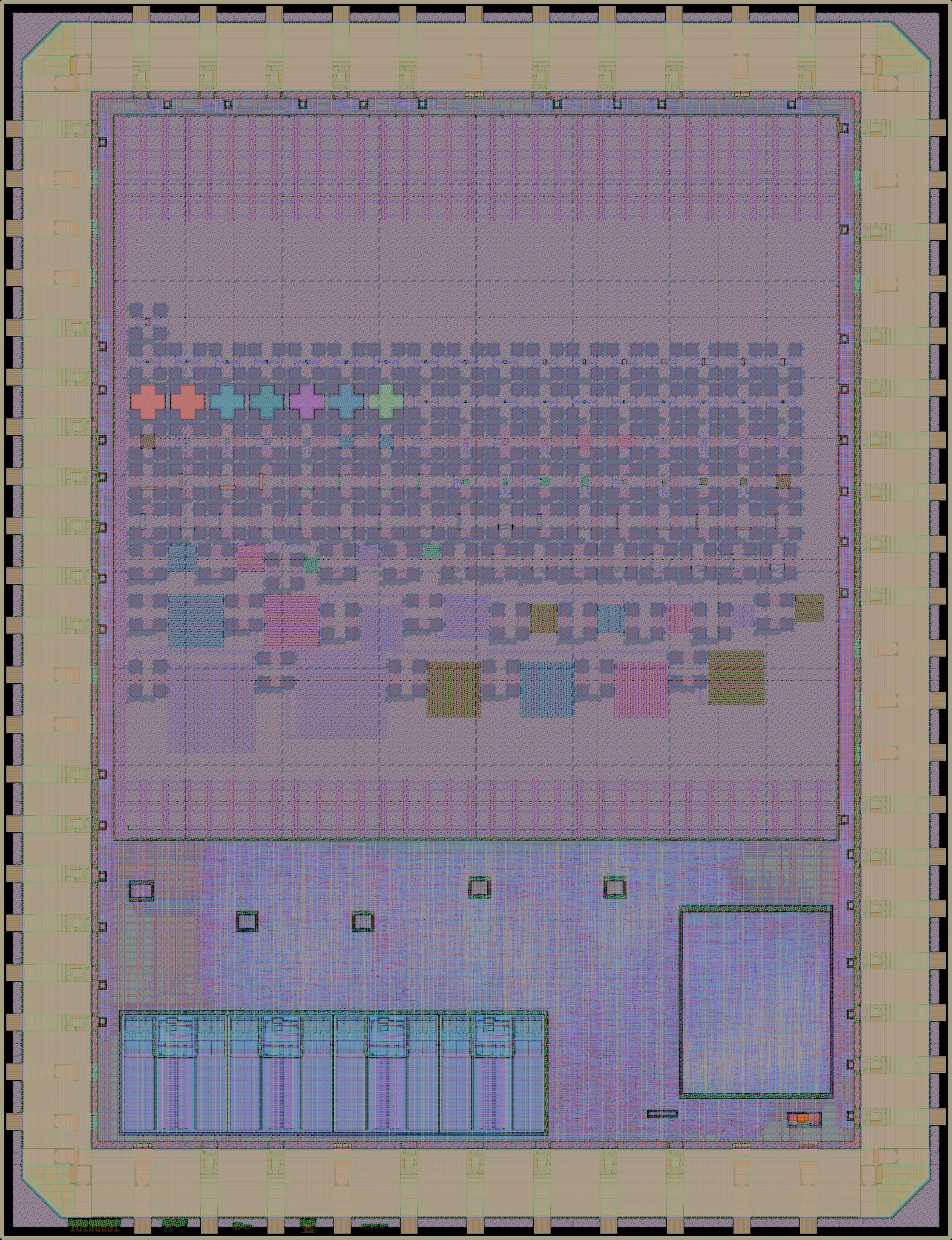
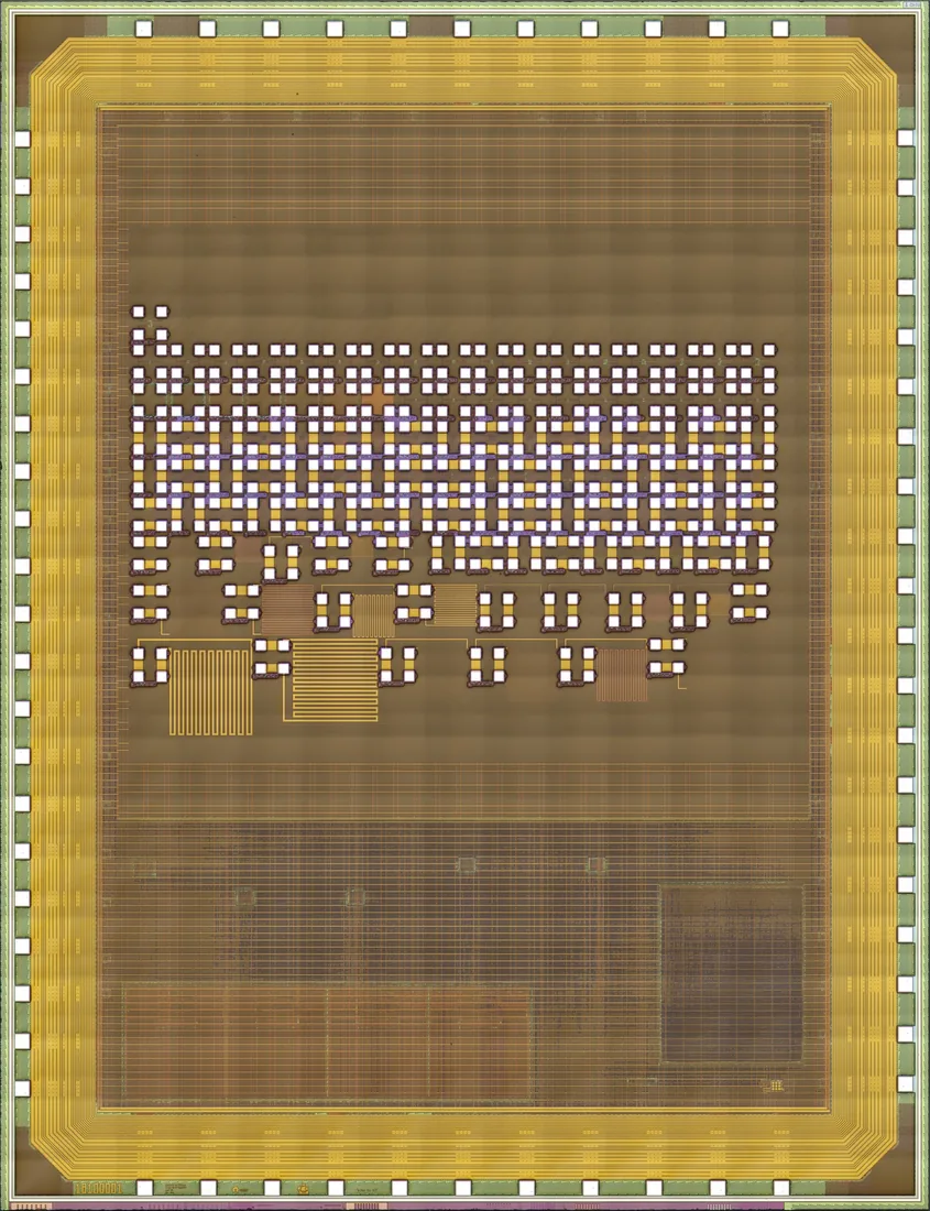
Rendered from the layout at 2.5 µm per pixel. Layers: NwellDiffusionPolysiliconMetal 1Metal 2Metal 3Metal 4Metal 5Top metalPad openings
Every figure here is measured from the public layout, the same way for every design on the run: see data and method, and how its designs used the process.
GF180MCU test structures by Philipp Gühring of LibreSilicon; Silicon Prawn identifies the die as LibreSilicon's Danube River test tile (https://gitlab.libresilicon.com/generator-tools/danube-river).
Source repository Die photographAs shipped
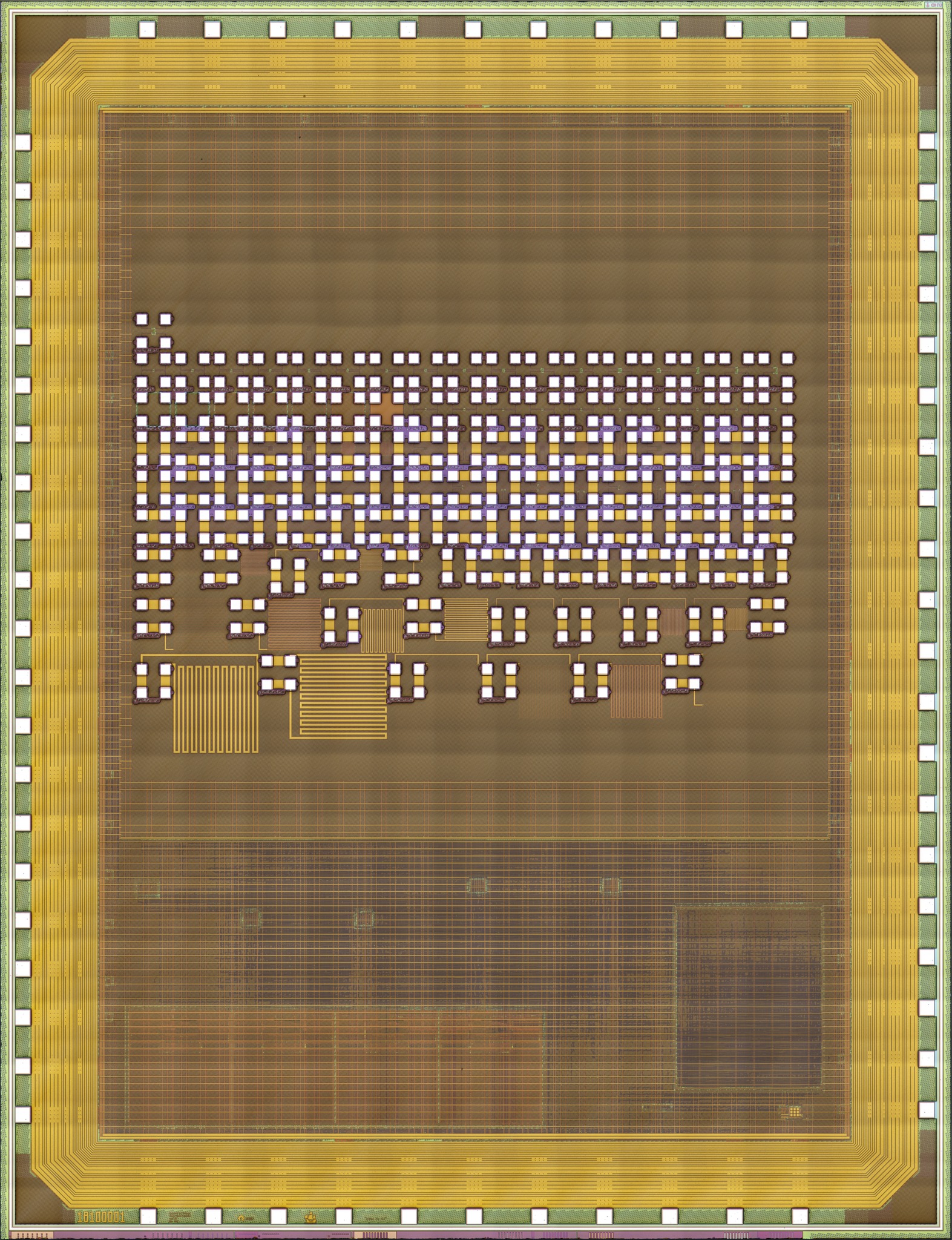
The fabricated die
A photograph of the finished chip, taken through a microscope after manufacture: optical micrograph © 2025 John McMaster, CC BY 4.0