Google GF180MCU open shuttle (GFMPW‑0) · Run by Google and Efabless
SkullFET
14FB · Analog and mixed-signal · 1 × 1 slot
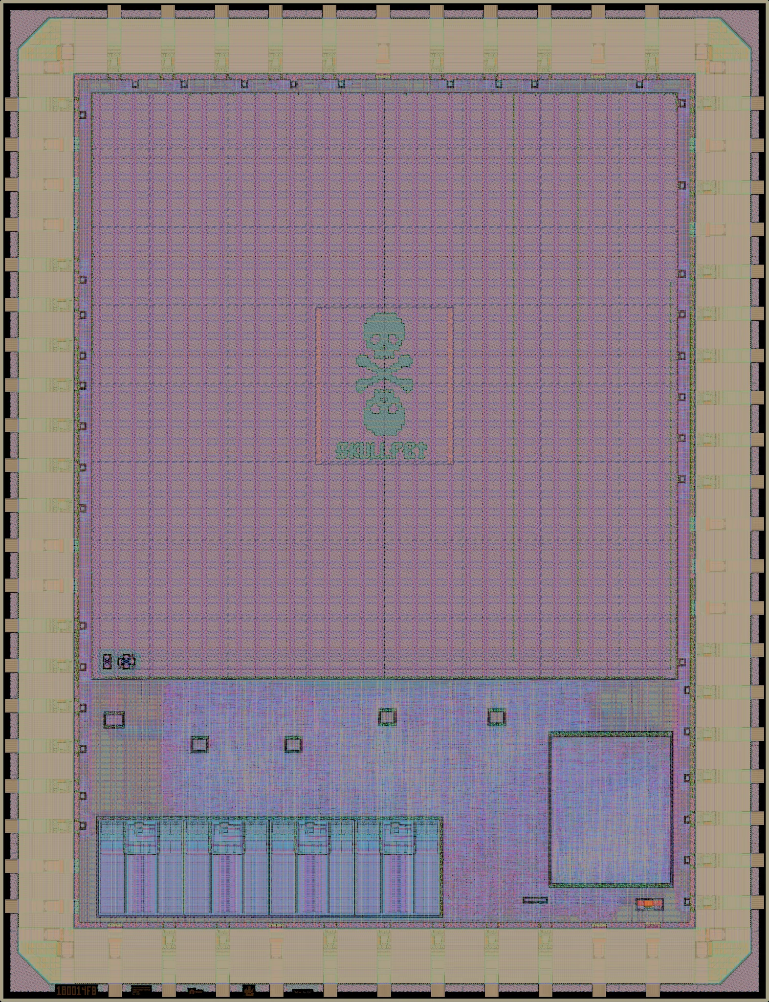
Rendered from the layout at 2.5 µm per pixel. Layers: NwellDiffusionPolysiliconMetal 1Metal 2Metal 3Metal 4Metal 5Top metalPad openings
Every figure here is measured from the public layout, the same way for every design on the run: see data and method, and how its designs used the process.
SkullFET barebone transistor cells (inverter, NAND). By Uri Shaked.
| Die | 3.93 × 5.12 mm (20.1 mm²) |
|---|---|
| Core area | 9.00 mm² inside the pad ring
its user_project_wrapper cell |
| Placements | 1 on the reticle, in slot E2 |
| Bond pads | 63 |
| Transistors | 6 |
| Logic cells | 0 |
| SRAM | No SRAM |
Process features
Which parts of the GF180MCU process this design uses: its transistor voltages and where they come from, its gate oxides, and any devices drawn by hand outside the standard cells, SRAM and pads.
| 6 V | 6 custom transistors |
|---|---|
| Gate oxides | Thick only (5 V/6 V) in the design itself |