Google GF180MCU open shuttle (GFMPW‑0) · Run by Google and Efabless
Signed 8-bit multiplier
A3A3 · Other digital · 1 × 1 slot
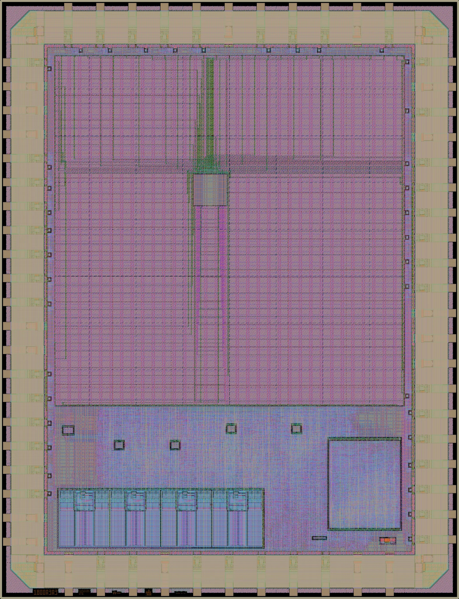
Rendered from the layout at 2.5 µm per pixel. Layers: NwellDiffusionPolysiliconMetal 1Metal 2Metal 3Metal 4Metal 5Top metalPad openings
Every figure here is measured from the public layout, the same way for every design on the run: see data and method, and how its designs used the process.
Signed 8-bit multiplier, alongside the VGA clock demo.
| Die | 3.93 × 5.12 mm (20.1 mm²) |
|---|---|
| Core area | 9.00 mm² inside the pad ring
its user_project_wrapper cell |
| Placements | 1 on the reticle, in slot B2 |
| Bond pads | 63 |
| Transistors | 16,376 |
| Logic cells | 0 + 2,385 filler and tap cells |
| SRAM | No SRAM |