Google GF180MCU open shuttle (GFMPW‑0) · Run by Google and Efabless
Universal gates
7F0C · Other digital · 1 × 1 slot
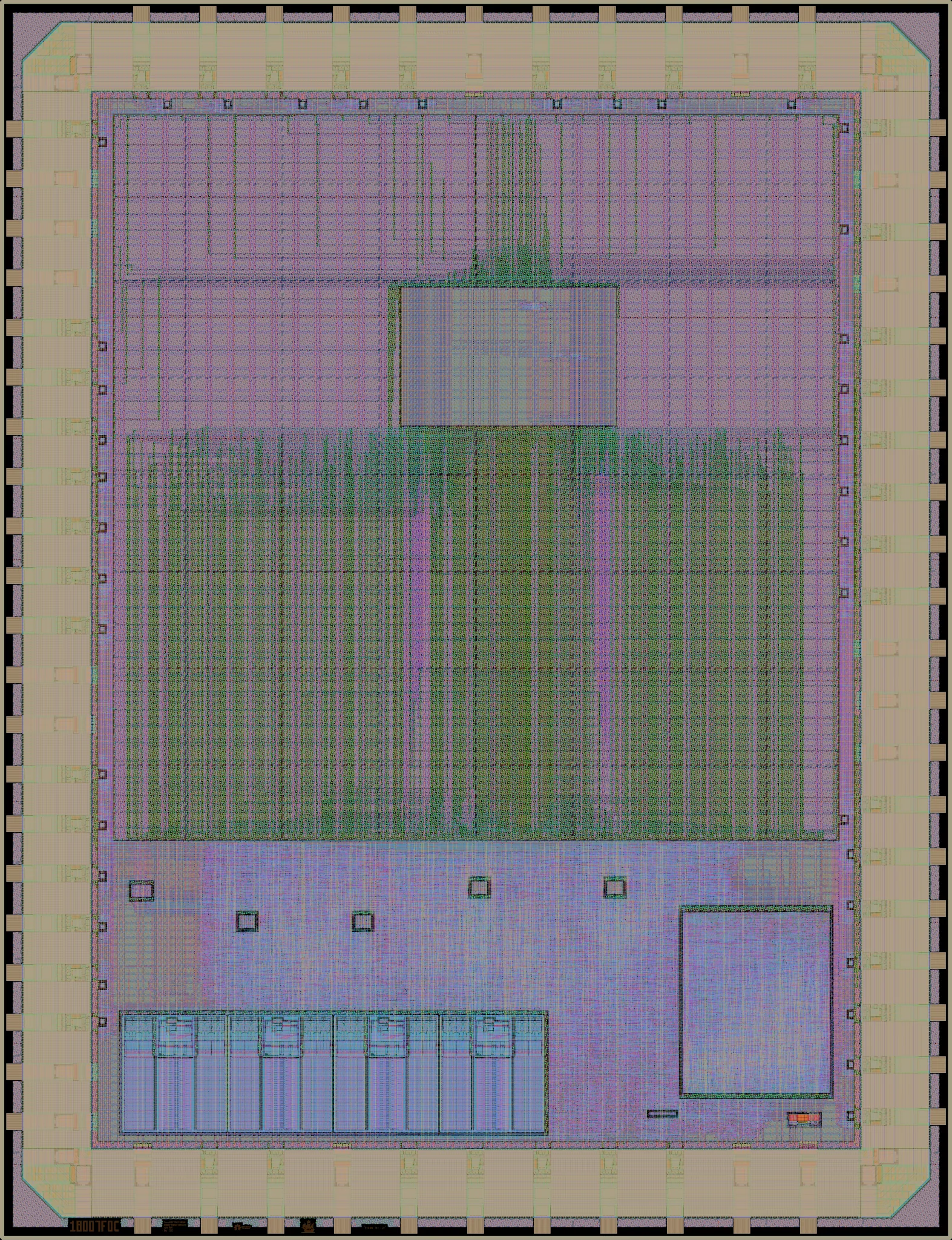
Rendered from the layout at 2.5 µm per pixel. Layers: NwellDiffusionPolysiliconMetal 1Metal 2Metal 3Metal 4Metal 5Top metalPad openings
182 logic cells: too few for density figures, which are given for designs of 1,000 or more.
Every figure here is measured from the public layout, the same way for every design on the run: see data and method, and how its designs used the process.
Universal gates: any 2-input Boolean function built from at most 5 NAND gates. By Tamas Hubai.
| Die | 3.93 × 5.12 mm (20.1 mm²) |
|---|---|
| Core area | 9.00 mm² inside the pad ring
its user_project_wrapper cell |
| Placements | 1 on the reticle, in slot D4 |
| Bond pads | 63 |
| Transistors | 109,489 |
| Logic cells | 182 + 14,489 filler and tap cells |
| Libraries | 7t-5V (182) |
| SRAM | No SRAM |
Process features
Which parts of the GF180MCU process this design uses: its transistor voltages and where they come from, its gate oxides, and any devices drawn by hand outside the standard cells, SRAM and pads.
| 5 V | 7t-5V standard cells |
|---|---|
| Gate oxides | Thick only (5 V/6 V) in the design itself |
Where the area went
How this design's area splits between filler and tap cells, other and outside the user area.
- Filler and tap cells 0.50 mm² (2%)
- Other 8.49 mm² (42%)
- Outside the user area 11.12 mm² (55%)
Most used cells
The ten standard cells this design uses most.
| Cell | Library | Instances | What it does |
|---|---|---|---|
| clkbuf_1 | 7t-5V | 53 | Clock buffer |
| clkbuf_3 | 7t-5V | 39 | Clock buffer (3x drive) |
| dlyc_1 | 7t-5V | 14 | Delay buffer |
| clkinv_1 | 7t-5V | 11 | Clock inverter |
| xor2_1 | 7t-5V | 10 | 2-input XOR gate |
| nand2_1 | 7t-5V | 7 | 2-input NAND gate |
| nor2_1 | 7t-5V | 7 | 2-input NOR gate |
| aoi21_1 | 7t-5V | 6 | AND-OR-Invert compound gate |
| buf_1 | 7t-5V | 6 | Buffer |
| xor3_1 | 7t-5V | 6 | 3-input XOR gate |