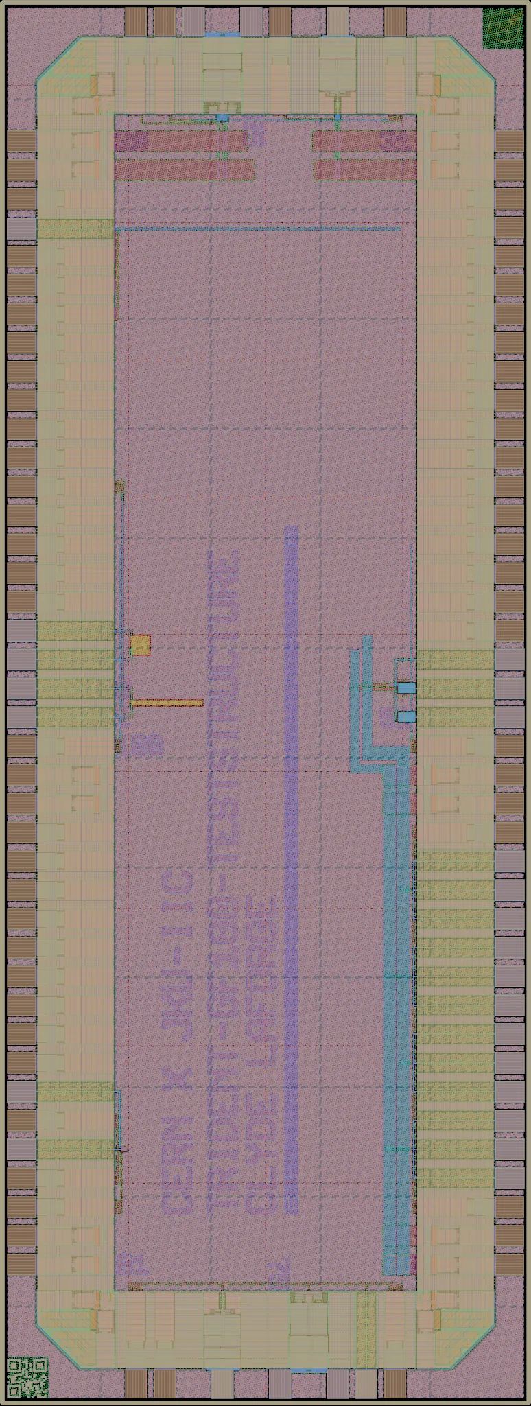
Rendered from the layout at 2.5 µm per pixel. Layers: NwellDiffusionPolysiliconMetal 1Metal 2Metal 3Metal 4Metal 5Top metalPad openings
Every figure here is measured from the public layout, the same way for every design on the run: see data and method, and how its designs used the process.
Test structures to evaluate leakage currents in gf180mcuD technology
| Die | 1.94 × 5.12 mm (9.9 mm²) |
|---|---|
| Core area | 4.47 mm² inside the pad ring
the project template's, 442 µm in from each edge |
| Inside the seal ring | 9.57 mm² (the die less its 26 µm seal ring) |
| Placements | 1 on the reticle, in slot H4 |
| Bond pads | 94 |
| Transistors | 20,114 |
| Logic cells | 0 |
| SRAM | No SRAM |
Submission
| Licence | CERN-OHL-W-2.0 declared
Repository: Apache-2.0 in LICENSES/Apache-2.0.txt, CC-BY-4.0 in LICENSES/CC-BY-4.0.txt, CERN-OHL-W-2.0 in LICENSES/CERN-OHL-W-2.0.txt, LPPL-1.3c in LICENSES/LPPL-1.3c.txt, LicenseRef-CERNLogo in LICENSES/LicenseRef-CERNLogo.txt — agrees |
|---|---|
| How it was checked | Commit and PDK pinThe licence and template were read from the repository at commit f81200d5f0b3. |
| Chip-on-board | Not selected at submission |
| Precheck | Passed
the check it was accepted on, 2026-01-03, gf180mcu-precheck 1.5.5 (from its image)
step results and logs |
Process features
Which parts of the GF180MCU process this design uses: its transistor voltages and where they come from, its gate oxides, and any devices drawn by hand outside the standard cells, SRAM and pads.
| 3.3 V | 12 custom transistors |
|---|---|
| 6 V | 8 custom transistors |
| Gate oxides | Thin (3.3 V) and thick (5 V/6 V) in the design itself |
| MIM capacitors | 2 (8,192 µm², between Metal4 and Metal5) |
| MOS capacitors | 40 (9,000 µm²) |
| High-resistance poly resistors | 36 (272 µm²) |
| Diodes | 276 (33,166 µm²) |
| Deep N-well | 12 (28,204 µm²) |
| I/O library | gf180mcu_fd_io (509 cells) |
Precheck
Before a design is made, the wafer.space platform checks it against the foundry's design rules. TRID was accepted on this check.
All 15 steps passed, with 0 KLayout DRC errors, on 2026-01-03.
Every step
| Step | Accepted on, and latest check 220, 2026-01-03, retry, gf180mcu-precheck 1.5.5 (from its image) PDK wafer-space/gf180mcu 1.6.6, LibreLane e2f0b0e |
|---|---|
| KLayout.ReadLayout | passed |
| KLayout.CheckTopLevel | passed |
| KLayout.CheckSize | passed |
| KLayout.GenerateID | passed |
| KLayout.Density | passed |
| Checker.KLayoutDensity | passed |
| KLayout.ZeroAreaPolygons | passed |
| Checker.KLayoutZeroAreaPolygons | passed |
| KLayout.Antenna | passed |
| Checker.KLayoutAntenna | passed |
| Magic.DRC | passed |
| Checker.MagicDRC | advisory warning |
| KLayout.DRC | passed |
| Checker.KLayoutDRC | passed |
| KLayout.WriteLayout | passed |
| KLayout DRC errors | 0 |
| Magic DRC errors (advisory) | 8 |
| Files | steps · log (gzip) |
The steps of the gf180mcu-precheck LibreLane flow, as run by platform.wafer.space. The design was accepted on the newest finished check before it was submitted; later re-runs check the same file with updated rules. KLayout DRC is the sign-off check. Magic DRC is advisory: its count does not stop a design. In the logs, Magic's "Error while reading cell" lines about fill cells are messages from its reader, not check failures.