Tiny Tapeout GF 26a · Die T26A on wafer.space Run 2
Stochastic neuron + STDP controller (merged, GF180)
358 · Other digital · 1 × 2 tiles
by Prof. Santhosh Sivasubramani, IIT Delhi
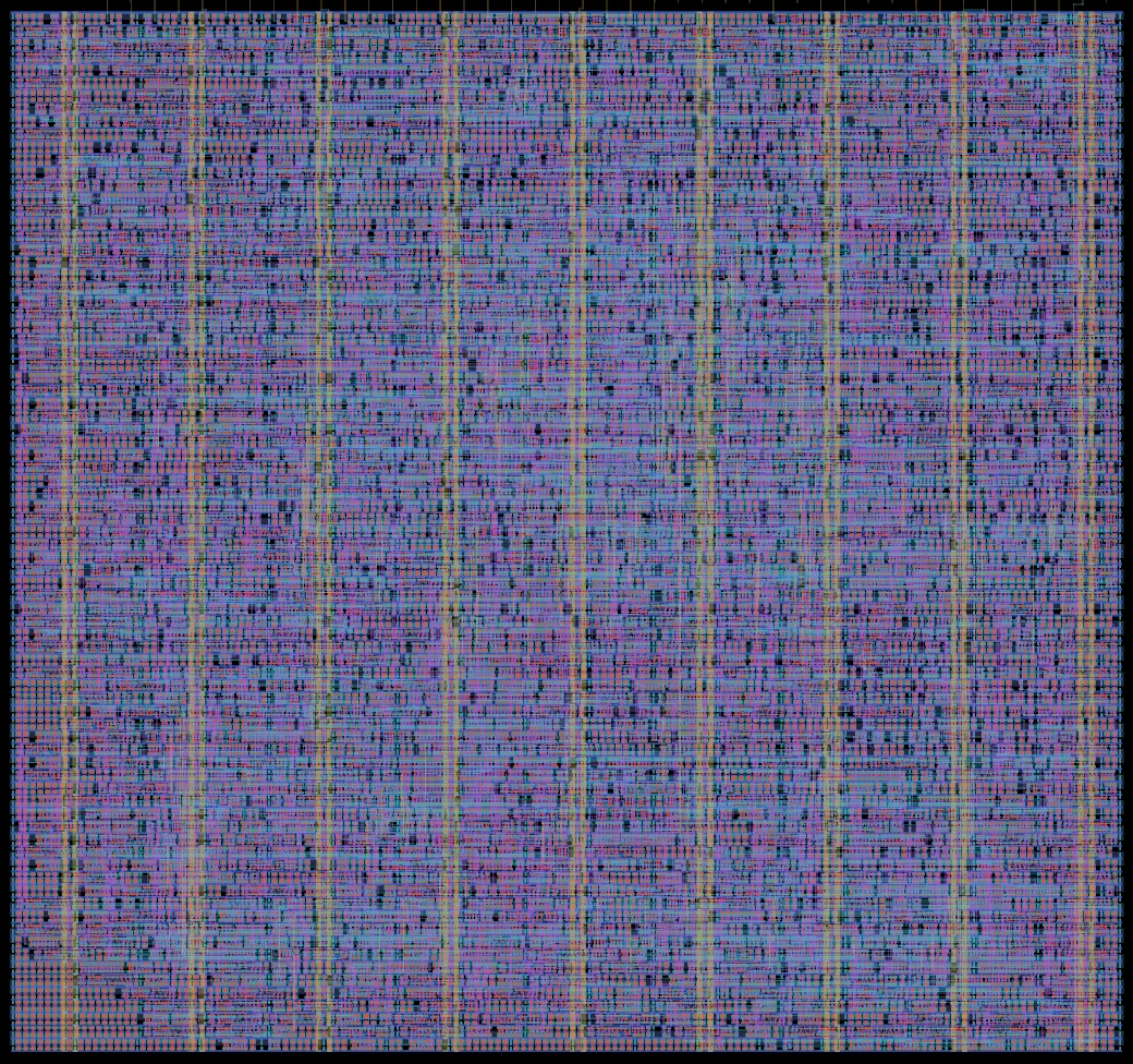
Rendered from the layout at 0.33 µm per pixel. Layers: NwellDiffusionPolysiliconMetal 1Metal 2Metal 3Metal 4Metal 5Top metalPad openings
Logic density
| Core average logic cells per mm² | 21k (28% of buffer maximum) |
|---|---|
| Densest 0.1 mm square logic cells per mm² | 27k (36% of buffer maximum) |
| Core covered by logic | 69% |
| Transistor density transistors per mm² | 299k average, 338k in the 0.1 mm square with the most logic cells |
Every figure here is measured from the public layout, the same way for every design on the chip: see data and method, and how its designs used the process.
GF180mcuD merged-pair cell: an 8-bit saturating LIF/stochastic neuron with an 8-entry sigmoid LUT, 8-bit Galois LFSR, programmable refractory, per-clock leak, host-triggered stimulus on ext_input rising edge, homeostatic theta adaptation over a 256-clock window (theta_live floats between theta_min and theta_max depending on spike count vs reg_target), and a 16-clock Bayesian confidence window emitting a 2-bit conf output. The second block is an STDP controller with 8-bit pre/post spike traces, per-clock exponential-shift decay (reg_tau_plus / reg_tau_minus), an anti-Hebbian polarity bit and optional reward-gated learning; on every LTP event (post spike with pre trace != 0) or LTD event (pre spike with post trace != 0) a 1-cycle weight_update pulse is emitted along with a learn_dir bit and a magnitude latch read over SPI. All registers are programmable via an 8-bit-data SPI mode-0 slave shared with the other TTGF26a tiles. 25 MHz signoff.
Source repository no longer public Its page on Tiny TapeoutBuy a chip and board
| Size | 347 × 325 µm (0.113 mm²) |
|---|---|
| Macro | tt_um_santhosh_stoch_stdp_pair_gf |
| Files | documentation · licence · layout and netlist in Tiny Tapeout GF 26a |
| Tiles | 1 × 2 at column 7, row 14 of the tile grid |
| Mux address | 358 |
| Language | Verilog |
| Clock | 25 MHz |
| Built with | LibreLane 3.0.3, open_pdks 54435919abff |
| Transistors | 34,534 |
| Logic cells | 2,435 + 3,670 filler and tap cells |
| Libraries | 7t-5V (2k) |
| SRAM | No SRAM |
Process features
Which parts of the GF180MCU process this design uses: its transistor voltages and where they come from, its gate oxides, and any devices drawn by hand outside the standard cells, SRAM and pads.
| 5 V | 7t-5V standard cells |
|---|---|
| Gate oxides | Thick only (5 V/6 V) in the design itself |
Where the area went
How this project's area splits between logic cells, filler and tap cells and other.
- Logic cells 0.08 mm² (69%)
- Filler and tap cells 0.03 mm² (24%)
- Other 0.01 mm² (7%)
Most used cells
The ten standard cells this design uses most.
| Cell | Library | Instances | What it does |
|---|---|---|---|
| dffrnq_1 | 7t-5V | 313 | D flip-flop with reset |
| mux2_2 | 7t-5V | 243 | 2-input multiplexer (2x drive) |
| nand2_1 | 7t-5V | 184 | 2-input NAND gate |
| buf_2 | 7t-5V | 146 | Buffer (2x drive) |
| dlyb_1 | 7t-5V | 146 | Delay buffer |
| nor2_1 | 7t-5V | 104 | 2-input NOR gate |
| clkbuf_2 | 7t-5V | 101 | Clock buffer (2x drive) |
| oai21_1 | 7t-5V | 100 | OR-AND-Invert compound gate |
| aoi22_1 | 7t-5V | 96 | AND-OR-Invert (2x2 inputs) |
| clkinv_1 | 7t-5V | 96 | Clock inverter |
Logic density map
Logic cells per mm² in each 0.1 mm square of the project (counted in the square, scaled up to a mm²). Hatched outlines are SRAM macros; the red outline is the densest 0.1 mm square that avoids them (27k logic cells per mm²), found by sliding a 0.1 mm square over the project in 20 µm steps, so it can straddle the fixed squares and find more than any one of them. Squares at the edges are partial, so they read low.
Tiny Tapeout and wafer.space are independent companies that work together (announcement). Tiny Tapeout runs its own shuttles: it takes the projects, builds the die, and sells and supports the chips and boards. wafer.space has the dies manufactured on its GF180MCU runs, and these pages are wafer.space's measurements of them. For anything about a Tiny Tapeout project, chip or order, contact Tiny Tapeout.