
A Need for Speed: Tholin's Own Standard Cell Library
Performance – an elusive metric that is influenced by everything the chip consists of, and more. The HDL that defines it, the way it is logically laid out, to the tiniest splattering of a chemical on the wafer, and the environment the chip lives in. How far can you go to chase speed?
PDK, SCL, WTH?
Current wafer.space shuttles target a 180 nm process provided by Global Foundries – they’re the people who turn your design into a real chip. A piece of the puzzle that allows this to happen is the “process development kit”, or PDK for short. A PDK contains everything you (and the tools) need to know in order to manufacture using their specific process.
An important component of the PDK is the “standard cell library” (SCL) – this library provides a set of fundamental building blocks that allow your chip to come to life. They can be anything from simple NOT gates to clock buffers and multiplexers. These standard cells are used by tools such as LibreLane to turn your circuit from a HDL of your choice, to something that can be etched and deposited onto a piece of silicon.
Standard cells provided by Global Foundries, from left to right: inverter, clock buffer and multiplexer
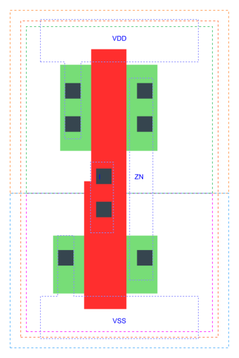
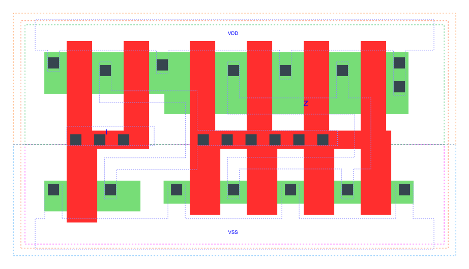
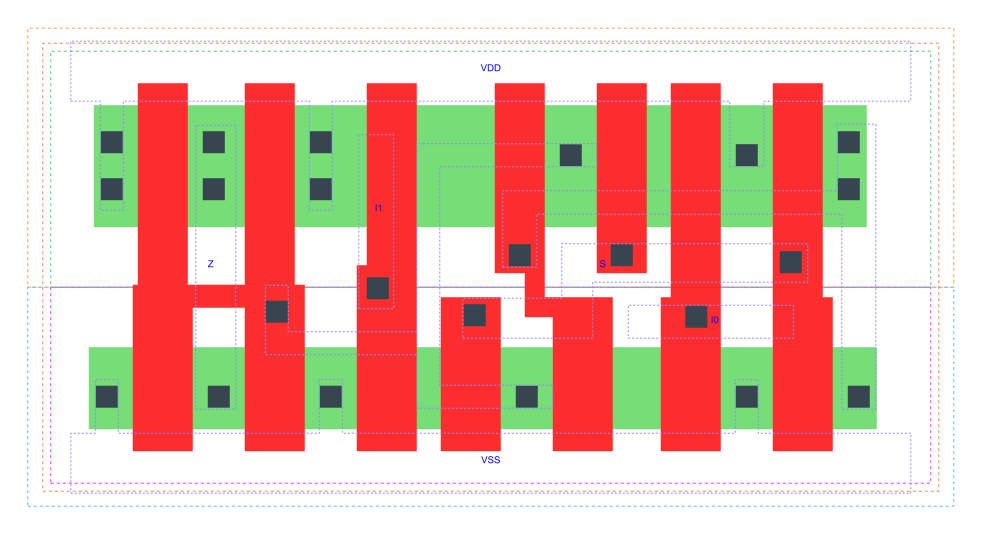
The PDK provided by Global Foundries (known affectionately as the gf180mcu_fd_sc_mcu7t5v0, or as GF180MCU) provides a
large collection of these cells, along with useful timing and process information. For many, this would be enough - a
simple, straight forward translation of a design into silicon using something provided by the creators of the process
themselves. Except… there’s a small snag: it’s slow. Their open source PDK targets 5 V, and therefore the standard
cells are made with transistors that are thick enough to handle this. Whilst they still can be run at 3.3 V, you still
suffer a performance penalty due to their size. This trade-off means you cannot squeeze as much performance out of your
circuit as you might want to, thanks to higher current requirements and threshold voltages required for thicker
transistors. So, what can you do if you’re after performance?
BYOSCL (Bring Your Own Standard Cell Library)
Tholin, of Avalon Semiconductors, posed this exact question. What was the answer? To create her own standard cell library that would deliver the performance she’d been after.
You see, Tholin has been developing chips for a while now – starting off with submissions to Tiny Tapeout’s TT02, she has now taped out various designs onto our Run #1 and Run #2 shuttles. Throughout these years however, she needed speed – in fact, she felt that no one had pushed the limits of what was possible with SkyWater’s 130nm (SKY130) process and decided to tackle the problem head on. Unfortunately, this didn’t lead anywhere but with some experience gained and important lessons learnt, she would be better equipped for next time.
After some turbulent events with eFabless shutting down and Google stopping their GFMPW programme, SKY130 was all that remained. That was until wafer.space entered the scene, and began to offer affordable GF180MCU shuttles, filling the void which had been left by the previous two. Tholin felt that GF180MCU had much more potential than SKY130, so she latched onto it pretty hard and dove right back into making her own cell library.
One Person, 102 Commits
Work began on June 30th, 2025. Five days later, the commit log reads “First working version”. 13 months of intense work
and 102 commits later, Tholin’s own gf180mcu_as_sc_mcu7t3v3 contains 85 placeable cells built entirely for 3.3 V
operation, along with characterization data.
| PDK | Cell | Voltage (V) | Delay (ps) |
|---|---|---|---|
| Foundry | inverter | 3.3 | 247.6 |
| Foundry | inverter | 5.0 | 184.2 |
| Tholin’s | inverter | 3.3 | 89.1 |
(Derived from the liberty timing tables shipped with each library at the typical corner (25 °C). Library level comparison, no real measurements so numbers remain theoretical.)
Despite the library not being 100% complete, it’s clear that there are solid performance gains to be had with a 3.3 V cell library. Tholin shares that in some metrics, it seems outperform her previous attempt at a high-speed SCL.
With the library taking up the taking up the exact same height as the default one, this can act as a drop-in replacement with a few simple tweaks to a config file.
If you want to explore the library, be sure to head over to its GitHub repository.
Building the Building Blocks
A lot of intense work goes into building a library of cells, even more so if you’re the only one working on it. Learning the practical knowledge, theory and best-practices takes hundreds of hours at best, but then you must also familiarise yourself with the various foundry-specific design rules and their nuances to ensure the cells can be manufactured in the first place.
Tholin shared her approach on how she created the cell library with us: “There is an absolute minimum number of cells you need to create before LibreLane accepts it at all: NAND, NOT, DFF, buffer, filler, tap, tie, diode. Once you have those, you can just add more logic cells as you see fit, in whatever order you want. I took a RISC-approach, synthesizing a RISC-V core with the fab SCL and checking which cells end up being used the most, recreating those first.”
Global Foundries' own inverter, open in KLayout
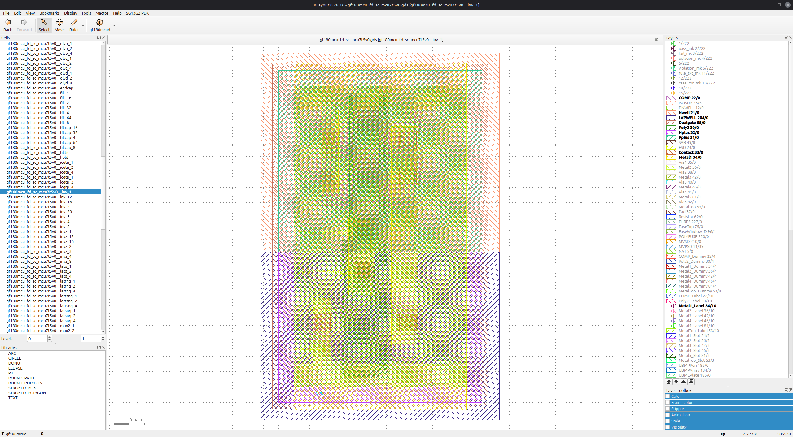
For those who might be unaware, you can build any logic function (AND, OR, NOT, e.t.c) you could wish for out of just NAND gates alone. They’re considered to be “universal gates” and so it makes sense that LibreLane would require it before any others. The filler and tap cells are used for the manufacturing process only.
Tholin's own inverter, open in Klayout
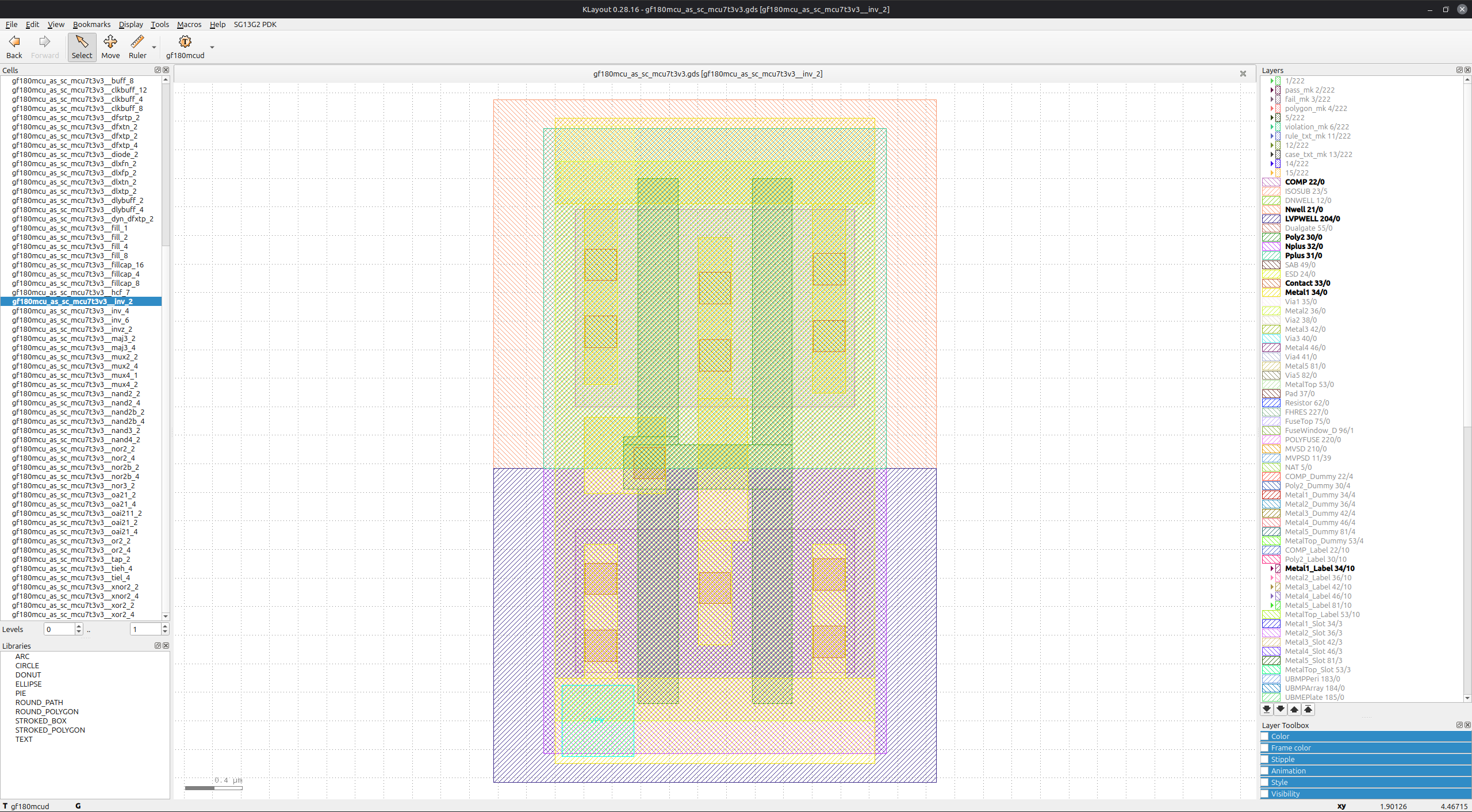
Tholin goes on to say: “As silly as it sounds, I use circuitjs for schematic capture and then go straight to layout. There is a lot of intuition, such as having memorized the relevant DRC minima until I got a “feel” for them. All cells must have the same height and a width that is a multiple of some unit width, and you have to be vigilant of potential DRC errors against adjacent cells, but its pretty free-form otherwise.”.
When asked about the work required to characterize each standard cell, she explains that “[c]haracterization is the part that usually takes the longest. That is running a thousand SPICE sims of each cell to figure out its DC and AC characteristics. Things like slew times and propagation delays are needed for timing analysis and repair. This process can be automated, but getting it set up initially with the right simulation parameters for each cell can take forever sometimes.”.
This library is important to Tholin, because not only does it provide something which the PDK was previously missing, but also because it pushes and legitimizes open source silicon as a real option for products, rather than being seen as a toy or an academic-only exercise.
What Does the Future Hold?
The library is only a few parts away from having a minimum set which Tholin is happy with. She explains that she’ll be able to focus on more specialized circuits such as full-adders and clock gates, or even experiment with DFFs which use the charge in the gate capacitance to store a bit – all in the name of performance.
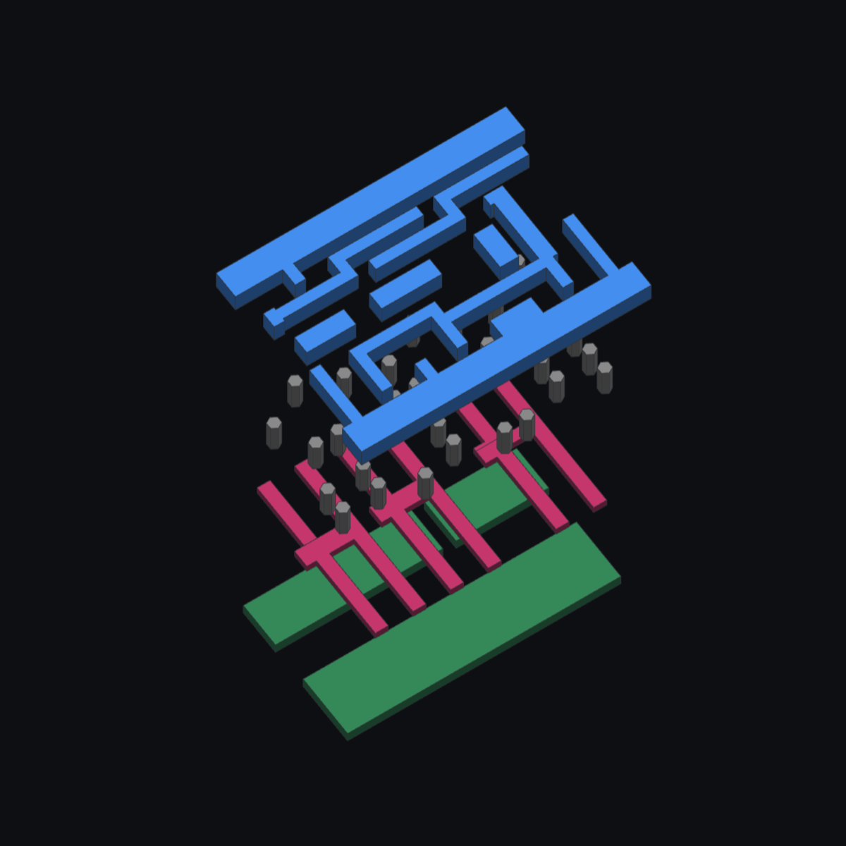
Render of Tholin's custom cell, courtesy of agentdavo.github.io/GDS3D/
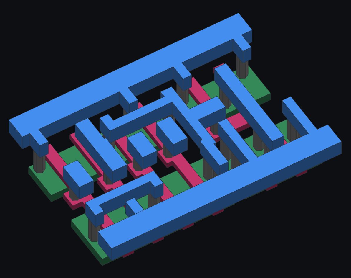
A stretch goal, she mentions, is compatibility with a tool called vlsiffra. This tool claims to generate “fast and efficient standard cell based adders, multipliers and multiply-adders”, potentially an excellent addition to the library and for those aiming to build fast processors or other computation cores.
The library is still very fresh, and not yet silicon-proven. What it means is that there is a non-zero chance that the chips might not be functional. We’ll only find out if all this hard work has paid off when Run #2 silicon returns from the foundry – if you’re considering using this library, you’ve been warned! Despite this though, people have already taped out designs which benefit from the extra speed such as Tholin’s own MPW, µTheia, FABulous FPGA and SlugTPU.
If you’re interested to hear about how all of this will turn out, consider joining the wafer.space Discord or Matrix.
A Message from Tholin
My background is over a decade of toying with electronic engineering as a hobby at a intermediate level with whatever parts I could get my hands on. I never made much headway in my professional career and I began doing chip stuff around November 2022, when I was 21 and getting bored of my web development job after 3 years. Never went to university, never formally learned anything about layout engineering, I just started doing chip dev projects during Tiny Tapeout 2 and never stopped for all this time.
A lot of people who see what I do tend to ask me HOW I got this far in a more abstract sense, since I’m almost a picturebook success story having dragged myself from nothing, no formal education, to 8+ tapeouts and two custom SCLs. So, here is some general advice I tend to give to people:
Just DO stuff. Like, that’s really it. I kept having ideas and kept doing them and now I’m here! The one rule is that you should always reach a bit higher than what you believe yourself capable off. I didn’t make an SCL because I had a precise plan of how to do it, I just found a starting point and began there, seeking out knowledge as I needed it. I actually ended up starting from scratch twice, but I learned a lot. Constantly stepping outside my comfort zone and falling on my face defined the whole journey, but you shouldn’t be afraid of that. Oh, and make sure your projects are things you care about. I never experienced a more painful burnout than the one time I took on a project just because “this would look good on my resume”.
You can find Tholin on Bluesky @tholin.bsky.social, read about her past projects on tholin.dev or see what she’s taping out in the wafer.space Discord.
Get Started Today
Run #3 is in full swing at the moment, so don’t miss your opportunity to tape out. You’ve got until 9 December 2026 to purchase a slot, and the submission deadline a week after on 16 December 2026.
Read more on our Crowd Supply page, jump in with our project template and join our community Discord to chat to other designers and get help.
